SSDs are surrounded by terminology that generally isn't understood beyond a relative level. There's this top-level concept that one type of NAND is superior to another, that synchronous is preferable to asynchronous, that endurance is tied to P/E cycles, but a lot of the knowledge halts there. We've worked closely with several SSD and controller engineers over the past year to educate ourselves on the inner workings of the storage world's biggest recent advancement; now it's time to start organizing that education in article form. Over the next weeks, we'll be releasing several "SSD Architecture" postings (so be sure to like / follow / subscribe) that focus on different aspects of solid-state drives, controllers, and NAND.
This installment includes a video component. The video showcases a discussion with LSI's Kent Smith and spoils the basics of what we'll cover throughout this series. I highly recommend watching the video, especially for those who benefit from visual aids. We covered SSD questions pertaining to varying voltage levels on evolving NAND types (SLC, MLC, TLC), cell decay when an SSD goes unused, P/E cycles and endurance, and "what's next" after TLC for Flash types. That's a lot of stuff. Each item is complex in its own way -- hence the chronicle-like release of in-depth article components.
Today we're talking about top-level SSD anatomy and architecture, defining what "NAND Flash" actually is, evolving NAND types (MLC vs. TLC, what's after TLC), capacity calculations, and providing an "SSD primer" of other basic elements. This is what will lay the foundation for our more advanced articles.
How Does TLC vs. MLC Work? P/E Cycles, Cell Decay, More
(Featured: Steve Burke, left, Editor-in-Chief - GamersNexus; Kent Smith, right, Sr. Director of Outbound Marketing for the Flash Components Division of LSI -- previously SandForce).
How is an SSD Made?
Just to give an understanding of where your SSDs come from, this video shows a previous tour of Kingston's SMT line (surface-mount technology):
What an SSD is Made Of -- Simplified SSD Architecture
SSD anatomy is more involved than mechanical storage on an electrical level, but isn't too terribly complex when it comes to the inventory of components found within each drive. The most noteworthy items of SSD composition can be broken down as:
- The Flash Controller.
- The NAND chips -- actual silicon that is responsible for data storage.
- Other active Integrated Circuits (ICs).
- Resistors, inductors, & capacitors.
- The actual SATA header / connector.
- An underlying Printed Circuit Board (PCB).
Most of the complexity exists within the controller and Flash memory, the rest is standard electrical engineering and circuitry to connect all the components. We'll move to the controller and NAND shortly.
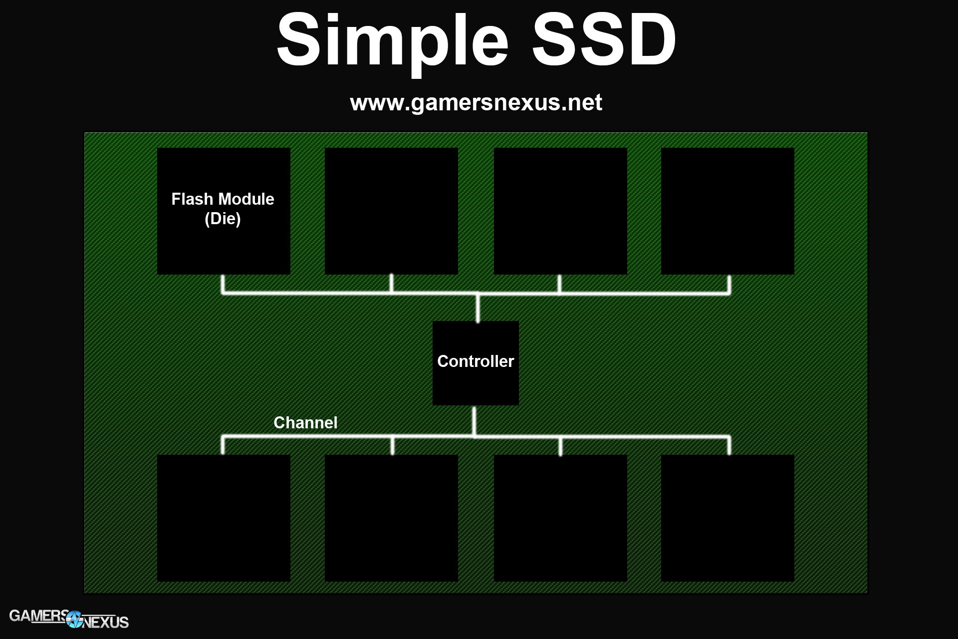
Let's look at an extremely basic sample SSD:
We've got a few core items in this simplified representation of a solid-state drive: The PCB (green), the Flash dies (black), and the controller (center, black). Stemming from the controller are eight channels, which effectively act as data pipes between the controller and Flash modules. Almost all modern SSDs host eight channels on the board, but not all SSDs populate those channels -- it is possible to only host six NAND dies and leave two channels unoccupied, for instance. Keep this in mind as we discuss SSD capacity and its impact on speed.
In our simple SSD above, we've got eight channels and eight flash modules. The NAND Flash modules contain your actual data and directly relate to capacity. Most SSD manufacturers -- Kingston, Crucial, Corsair included -- do not fabricate their own NAND Flash, but instead buy it from large Flash suppliers. These Flash suppliers are the very same fabrication facilities that produce DRAM modules, and include the likes of Micron (in partnership with Intel), Samsung, and Toshiba. Each fabricator has a different take on NAND Flash architecture and design, so there's no guide to be written that will give absolute, definitive rules as to the design of every NAND module made. That said, the basics remain constant throughout the consumer side of the industry; we only really start seeing significant differences in architecture once entering the Enterprise space, which is the very same space that drives innovation in new fab processes.
Before delving further into SSD architecture and capacities, let's talk about what a NAND module actually is on the inside.
A Primer on Flash Memory - What is "NAND Flash?"
NAND Flash memory can be seen as sort of an opposite of RAM (Random Access Memory), which—as you all know—is a type of fast, volatile memory used for storing data temporarily. In a gaming application, RAM is often used to store things like map data or variables within the world. Take Skyrim: We load most of the current cell's open world data and game functions into RAM to reduce the number of hits to the hard drive, which is significantly slower and would introduce noticeable load times. Every time you see a load screen in a game (or a 'lag spike' upon changing cells), it's generally a hit to the hard drive creating that downtime. In its most simplistic form, this is when the game calls for a dump of unneeded items in memory and calls for new data to be fetched from storage. RAM reduces the speed deficit of slow storage, but isn't always a viable programmatic solution -- that's why we recommend SSDs to mitigate downtime when storage must be accessed.
The word "Volatile" has special meaning as it relates to any type of electrical memory and serves as an indication of whether the device can retain its storage when power is lost. Non-volatile memory is represented in "permanent" storage -- hard drives, solid-state drives, and Flash memory ( USB, SD ) devices. Volatile memory is incredibly fast in its operations and is tied directly to the CPU and its integrated memory controller (IMC), eliminating the need to hit the physically-farther and slower storage device constantly. Volatile memory is so-named because it cannot retain the data once the unit has lost power, so it is 'wiped' and re-used regularly. A reboot will wipe all volatile memory. There are some exceptions that work around this, like RAMDisks, but those are outside of the scope for this article.
To best visualize volatility in memory, a rendering example is useful: When editing a video in software, the video editor is capable of performing a "RAM preview" before rendering out the content (writing the content to disk). In a RAM preview, the software loads all of the video data into RAM, or as much as will fit, and then accesses RAM for smooth playback without ever requiring a write or read from disk. Considering RAM hovers in the 12+ GB/s range for throughput and most HDDs are closer to 50MB/s sustained, the speed difference is enough to smoothly play high bit-rate video without lag.
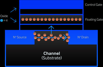
Both Flash memory and system memory (RAM) utilize NAND ("Negated AND") logic gates, which effectively control the flow of information throughout the device. These NAND gates are the reason we can write to and read from the modules. You can read in great depth about logic gates and NAND gates in the linked locations, though that's more of an electrical engineering topic and exits the top-level enthusiast scope of our website and article.
Flash memory was originally based on EEPROM, or Electrically Erasable Programmable Read-Only Memory, and has been adapted for use in modern SSDs. If you're familiar with the term "P/E cycles" -- or Program/Erase cycles -- as it pertains to SSDs, you'll already have a basic understanding of what "electrically-erasable / programmable" means. I'll define all of this below if I've lost you (quickly: P/E cycles represent the number of times data can be written to and erased from the Flash module before it is electrically depleted).
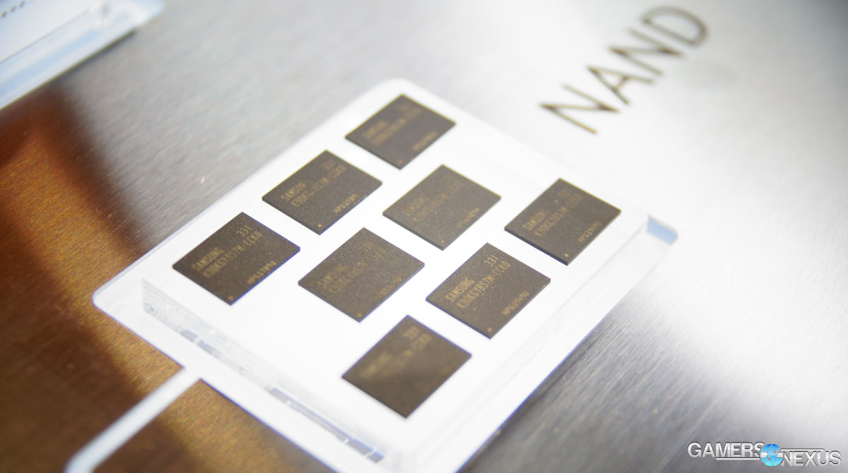
If you were to take apart your SSD and look at the components housed within the casing, you'd find a host PCB, the connectors, a controller (labeled 'SandForce,' 'Samsung,' etc.), and several black modules mounted to the PCB (normally in groupings of 2 or 4). The black modules mounted in clusters are the NAND Flash modules, which ultimately contain your data.
Continue to page 2 to learn about SSD capacity derivation, NAND architecture, channeling, and the impact on speed.
SSD Capacity, Channel Population, and Impact on Speed
Let's talk about the anatomy of a NAND Flash module and its impact on storage capacity. This is where the different fab processes and facilities can differ, but we retain overall standardized terminology and fundamentals across the consumer-class of SSDs. I'll be using Micron's newest 16nm MLC Flash NAND process as an example for this section, which is the very same NAND being used in Crucial's affordable SSDs that were released just recently.
Breaking down that name is a good starting block: "16nm MLC Flash NAND."
16nm - The "fab process" or physical size of the features on the silicon. This is regularly seen when discussing new GPUs and CPUs, like the jump from 32nm to 28nm process. The number is indicative of the smallest silicon incision on the semiconductor that the factory can make (think of this as a "cut" or "slice" of silicon). The size is normally directly correlated to the length of the gate for MOSFETs.
MLC - The NAND Flash type, which we'll define next in a large, separate section. These are often listed as "MLC" or "TLC" in consumer SSD applications, but also exist in "SLC" form for expensive Enterprise uses. The future of NAND includes 3D NAND (or VNAND), covered more in depth in the NAND Flash Types section below. "MLC" stands for multi-level cell, TLC for triple-level cell, and SLC for single-level cell. Again, the precise meaning of these words will be explored shortly.
With that defined, we can move on to channels, dies, and capacity calculations. Here's another very simple graphic using Micron's 128Gb Flash:
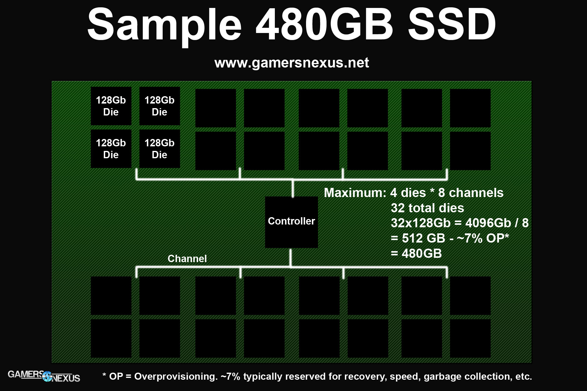
In this one, we've split the Flash dies into four pieces. Most modern controllers (like Gen3 SandForce, the newest Samsung controllers) operate at peak performance when speaking to a maximum of four dies per channel. We've got a fully-populated channel and controller configuration here, so the hypothetical Flash controller will be under maximum spec.
Capacity is measured in gigabits (Gb) for Flash and DRAM modules. There are eight bits in a byte, so 128Gb is equal to 16GB (128 / 8 = 16). With eight channels and four dies per channel, we've got 16GB * 4 dies * 8 channels = 512GB. You'll notice that the image is labeled as "480GB SSD," though, so we've got 32GB missing. That's because all SSDs reserve some of the Flash for "overprovisioning," which I've previously discussed in-depth here and here, in the SandForce Gen3 announcement. The industry average for consumers is about 7% overprovisioned space, but this varies greatly depending on a particular drive's target user.
We're not going to dive too deep into overprovisioning in this post -- mostly because I've already done it -- but will save that for the next article in the series. I don't want to make things too overwhelming in part one.
The very short of it is this: Overprovisioned (OP) space is used for background "swapping," part of the wear-leveling and garbage collection processes, and ensures extended life of the SSD. The overprovisioned space on modern SF Gen3 controllers (and presumably the impending Samsung controllers) can also be "called into action" from the reserves when part of the NAND goes bad. A single bad block can render an entire SSD useless, so this sort of "back-up NAND" that is reserved in OP would champion error-heavy blocks and continue operating normally. Using SMART attributes, we are able to determine once this call to the reserves has happened. It is always advisable to replace the device immediately after the reserve begins seeing use.
With our hypothetical controller being fully saturated on its eight channels with 32 dies, speed, efficiency, and capacity will be at their maximum spec. Because NAND is now being fabricated at the 128Gb capacity, it is likely that the cost of 480GB SSDs will drop as they become more desirable and standardized in the industry; we saw this same shift from 120GB to 240GB just recently. The reason 64GB SSDs have largely vanished is tied to the NAND capacity: it is no longer cost-effective for manufacturers to make 64GB SSDs, especially given the decrease in performance with fewer dies on the PCB. A 64GB SSD with 128Gb Flash would be 4x128Gb dies, not even a quarter of the maximum channel saturation of a modern controller. The controller would be hamstrung.
But there's a lot more to it than this.
What's Inside the NAND Flash Module - Planes, Blocks, & SSD Architecture
Here's another graphic I made to aid this discussion:
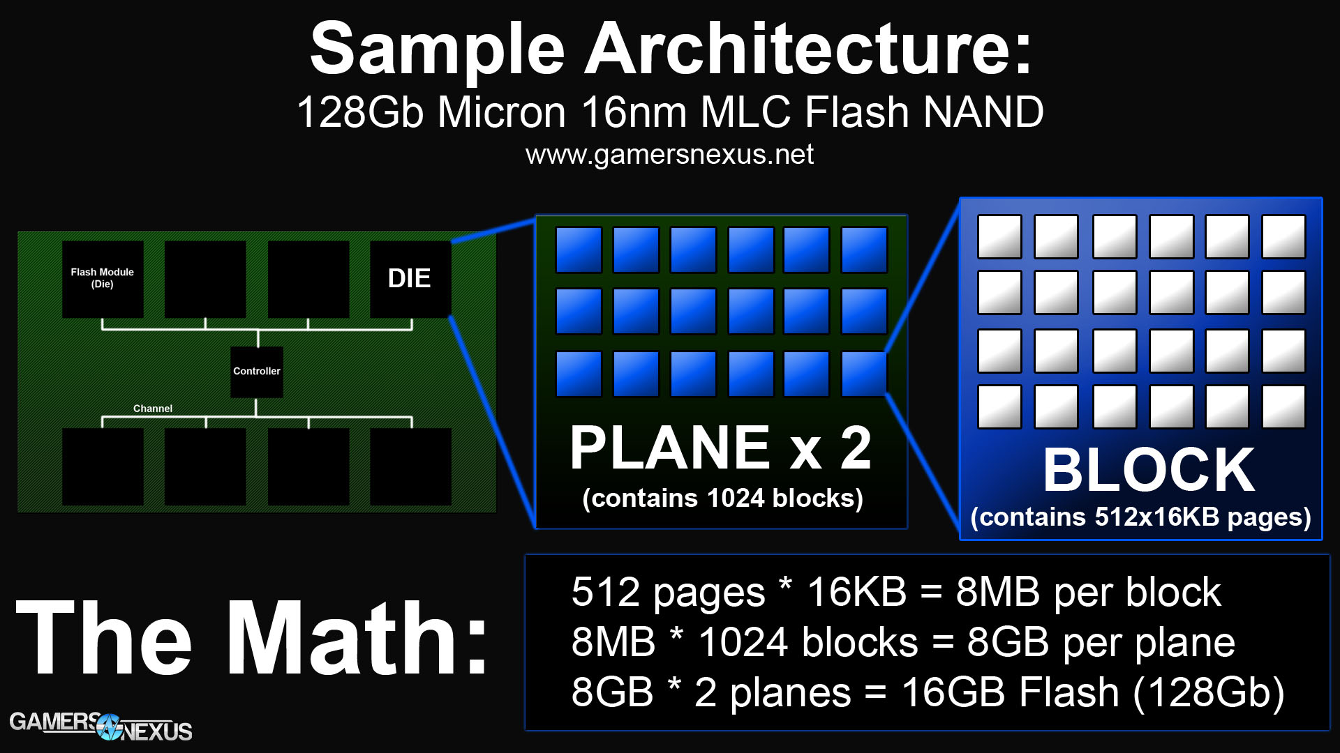
The green SSD makes a return, but this time, we're looking inside its components. We're still using Micron's 16nm, 128Gb Flash in this example. You'll see that the black blocks still represent Flash modules, but now we're expanding one into a "plane," which is then expanded into a "block," then expanded into "pages." This is how an SSD organizes its data storage.
Micron's NAND we're referencing uses a dual-plane architecture, so it's got two planes per die. Each plane hosts 1024 blocks, and each block hosts 512 pages that are 16KB large. If you do the math here, that's 512 pages * 16KB capacity = 8MB per block; 8MB * 1024 blocks = 8GB of data per plane; 8GB * 2 planes = a 16GB die, or 128Gb. This is then multiplied by the number of dies present on the device to achieve the capacity. Using our previous 32-die sample SSD, that'd be 16GB * 32 dies = 512GB, minus overprovisioning to equal 480GB.
This organization structure is a requirement given the way SSDs operate. NAND storage is handled electrically, so the modules have a limited lifespan measured in program/erase cycles (P/E). The NAND begins to lose its charge as the device ages, eventually sending voltages to the gates that can be "misinterpreted" as the incorrect voltage level. This is the catalyst for a "bit error." Error Checking & Correction (ECC) can resolve a number of bit errors, but once bit errors become a commonality, the NAND inevitably enters a locked, read-only state. This state is preserved for a set amount of time to allow for data retrieval (depends on manufacturer), after which point the SSD will shut off for good.
That's where it gets problematic without a controller-based solution. SSDs can only write in pages, which are measured at about 16KB in modern architecture. This means all of your data is broken into 16KB chunks (or smaller) and written to "pages" within a block on the NAND. The controller can later move this data around as it sees fit as a part of its wear-leveling and garbage collection processes. Even though an SSD can read from and write to small, 16KB pages, it can only erase entire blocks at a time.
Once any single block has been erased a total number of times that exceeds the lifespan of the NAND, that block is effectively electrically dead; a single dead block can render an entire SSD useless. Luckily for us, there are means to prevent uneven usage of an SSD and stave electrical death. Controllers use "wear-leveling" as a means to ensure all blocks are programmed and erased at an equivalent pace, which looks something like this:
This graphic shows a page being moved around within a block (left). In magnetic storage, the disk writes in an outward pattern from the center. This is because there is a physical header that must move around a spinning platter, so keeping data closer to the center makes it physically more accessible to the header as it seeks, increasing performance. With an SSD, it doesn't matter where the data is stored because it's all accessed electrically; this is the same reason fragmentation does not exist on an SSD, and is why an SSD should never be defragmented.
Remember that SSDs can only erase entire blocks at a time, so to make most efficient use of the P/E cycles, it doesn't make sense to erase a block that's only got a few pages on it. This is where wear-leveling comes into play by rotating the pages across blocks to ensure more even distribution as the device is programmed and erased. Some SSDs will advertise as having "3K P/E" cycles (take this HyperX 3K example), which means that the NAND is rated for 3,000 programs and erases before it exits spec and enters "use at your own risk" territory. To put things into perspective, most users will exhaust the usable life of the system before an SSD of similar endurance is depleted.
Continue to the third and final page to learn about NAND Flash types, how MLC & TLC work, and what comes after TLC.
Evolving NAND Flash Types: What is TLC? MLC? How Does TLC NAND Work?
So we've dissected the NAND Flash modules.
NAND Flash types often appear in marketing text as a sort-of battle of TLC vs. MLC. Both have their advantages and disadvantages, as with any technology, but a whole helluvalot more goes into SSD selection -- like the right controller, which can seriously impact the life of a drive. We'll get to those choices soon.
SLC was the first type of NAND readily available on SSDs (primarily enterprise); it's known for high endurance (10k, 20k, even more P/E cycles), performance, and its unattainable price for consumers. SLC devices heavily dominate the enterprise market where high-reliability and uptime are critical to success (web servers, database servers). MLC and TLC have made their way into the consumer market as more affordable options.
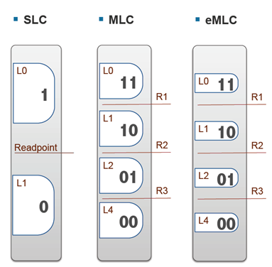
SLC stands for single-level cell, MLC for multi-level (two) cell, and TLC for triple-level cell. All of these acronyms are representative of how many bits of data are stored per cell and how many voltage levels are stored per cell. The different NAND types impact your cost-per-GB, total capacity, speed, and endurance of the device.
That's the rapid primer. Another one of our graphics should help out:
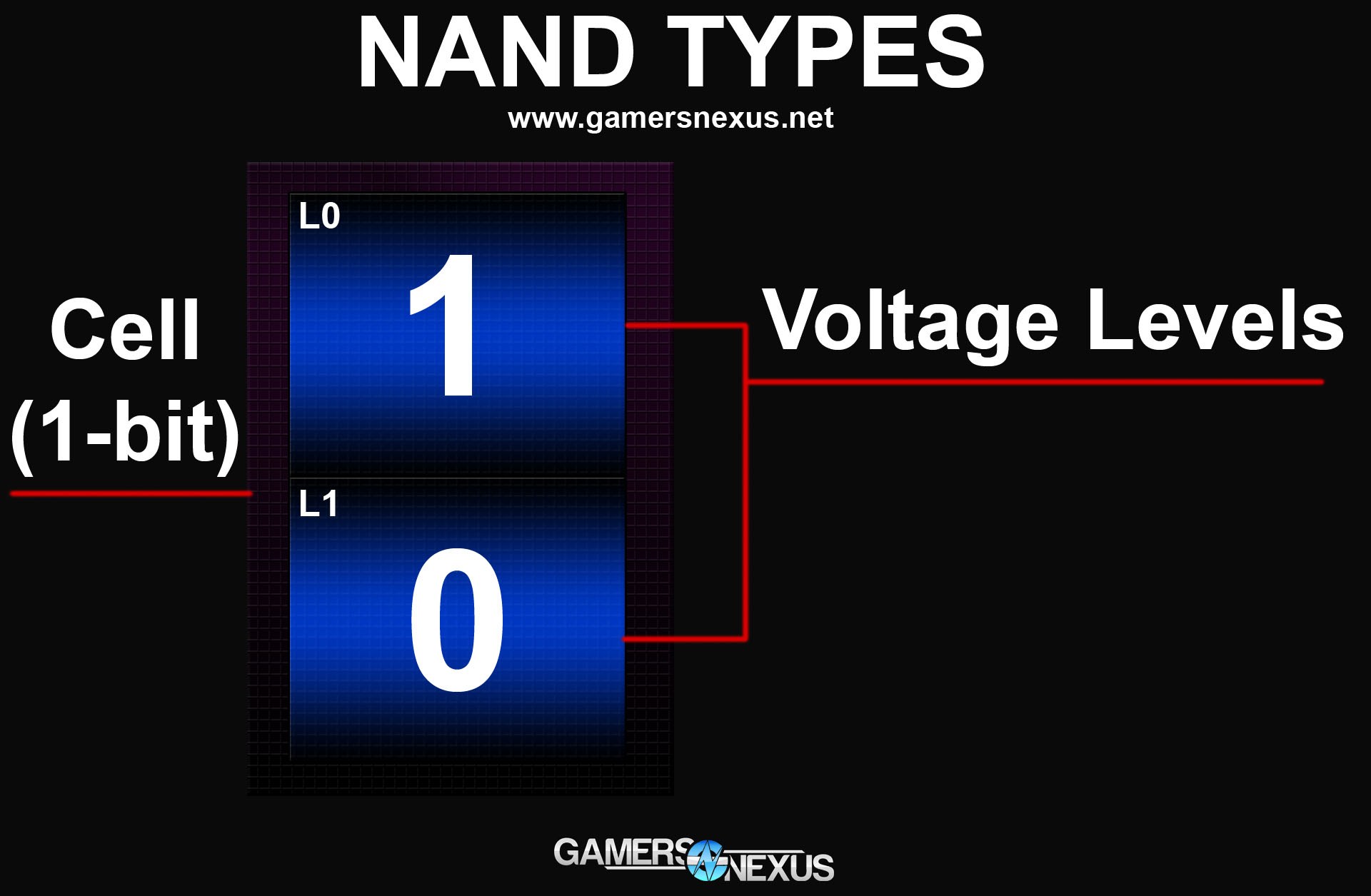
Meet a sample single-level cell. This cell can store a single bit of data, but that's OK, because there are typically billions of cells per SSD. In the above SLC sample, we've got two possible voltage levels for the cell: 1 and 0 -- binary. When a charge is sent to the cell, it returns either a 1 or a 0 for the voltage check. Because there are only two possible voltage outcomes, the device runs with greater stability and performance than the more populated multi-level and triple-level cells, each of which stores exponentially more voltage levels and requires greater electrical precision at the time of checking.
More voltage levels make for a slower device given the added complexity, but also make for increased possibility of error when checking the voltage of a cell. When the voltage level is misinterpreted, a bit error is thrown and stability is potentially compromised. Controllers mitigate this significantly, as I've explained above, making TLC and MLC viable consumer options. The stability and performance downsides are largely outweighed by affordability and capacity in consumer use cases, and because consumers don't hammer drives to the extent servers do, the downsides don't necessarily impact the majority of users.
Here's what MLC and TLC look like:
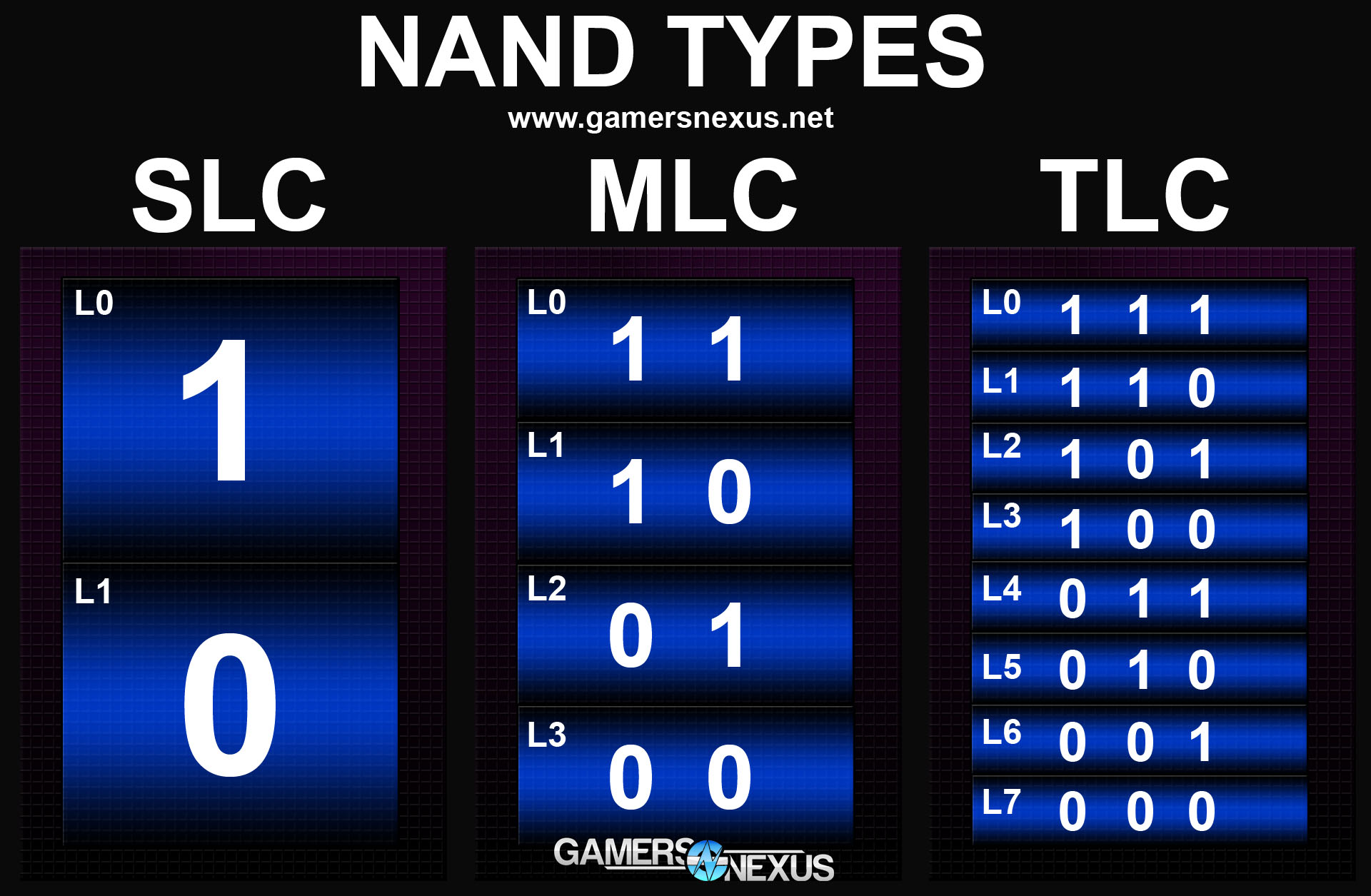
MLC contains two bits of data per cell and hosts four voltage levels; TLC contains three bits of data per cell and hosts eight voltage levels -- it's exponential (2^1, 2^2, 2^3). At three bits of data per cell, each cell offers significantly more capacity than SLC and MLC counterparts (3x SLC, ~30% more than MLC). This means the cost-per-GB can be reduced because less physical hardware is required to store more data, resulting in the affordable SSDs we've got on the market today. Higher die yield also impacts price.
Here's another look at voltage levels:
As Kent Smith describes with hand motions in the video, there are different "readpoints" between the voltage levels on the cell. SLC is definitive: One readpoint between level 0 (L0) and level 1 (L1). MLC features a readpoint between each of its four voltage levels, so three total readpoints. TLC (not shown, as this is an old graphic) would feature 7 readpoints. The more readpoints we cram into a cell, the more granularity required at the electrical level (voltages) to accurately check the bit; more granularity in the same amount of space means more room for error. Because we're fitting more bits onto a cell, the individual cells will take more of a beating (accessed more frequently) than the single-bit SLC counterparts, which impacts endurance. The electrical charge stored weakens as the device ages, the NAND gets "worn out" from being hammered for more bits per cell, and the SSD "dies" much sooner.
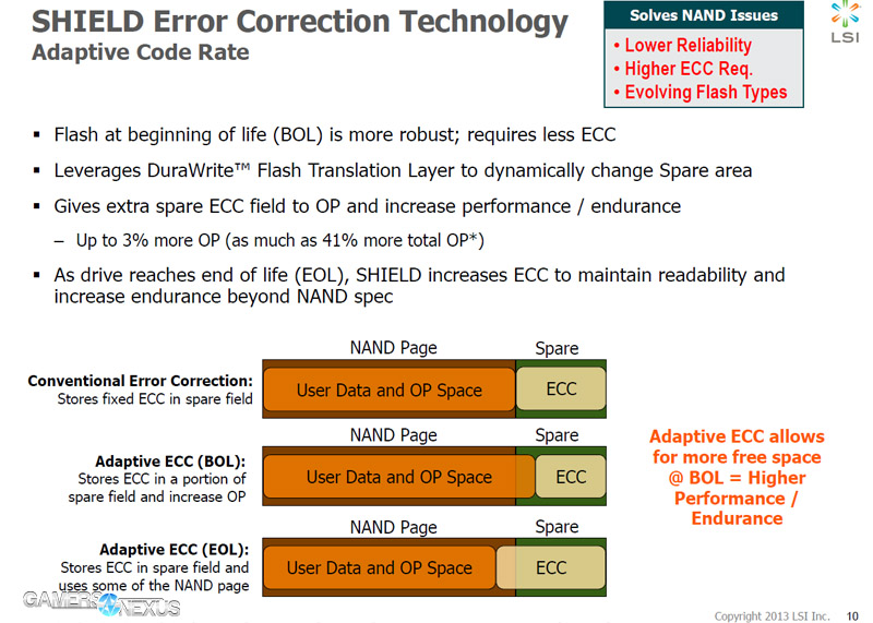
Controller manufacturers have implemented ways to mitigate this, like increased overprovisioned space with the "reserve NAND" I described above. Other means of reducing impact to the NAND include decreasing the Write Amplification Factor (WAF), which we've explored in depth previously. By downsizing WAF to below 1x, all data written to the device is heavily compressed and causes less negative impact to endurance. SandForce calls its version of WAF reduction "DuraWrite," which reduces data written to the flash. SandForce Gen3 will introduce "SHIELD" technology to its devices, which is an error correction method that pulls from overprovisioning to perform more error correction as the device ages.
The reason I point all of this out is to remove some concern of endurance as a consumer. Although there are very clear disadvantages to Flash types that store more bits per cell, the advantages and affordability outweigh those when coupled with a reliable controller. Most users in our audience will not deplete an MLC SSD before upgrading the system entirely, and the same goes for TLC. The performance hit is less noteworthy than endurance, but that's strictly because SSDs brush up against the SATA interface limit to begin with; it'd be more noticeable on an SSD using a faster interface.
What's Next for NAND: VNAND & 3D NAND
Just before CES 2014, Flash and DRAM manufacturer Samsung announced its plans for "3D NAND" as a next step after TLC. This isn't something we'll see any time soon in the consumer market, but it is worth talking about in preparation for the day.
The trouble with TLC is that it's packing so many bits onto a cell that endurance and stability are threatened. Accuracy with voltage levels is more of a concern, thermals are more of a concern, and speed is more of a concern. To resolve this, Samsung has proposed that NAND should be stacked vertically ("3D NAND" or "VNAND), distantly similar in concept to Intel's 3D transistors. This is analogous to real estate in heavily-populated areas: An apartment rise will fit more residents in a square area than single-family homes. Samsung even uses this analogy in its own video, found here:
It's still far too early to discuss the architecture and storage/endurance implications of this technology, so we'll leave it there.
SSD Death from Disuse
Watchers of our initial video may have noticed that death from disuse was a very brief discussion point. As an SSD ages and depletes P/E cycles, its charge and ability to differentiate between voltage levels also decays. Setting a moderately-to-heavily used SSD on a shelf for a year without use may result in data loss at next access, especially if the device has entered its read-only state after P/E cycle depletion. Kent Smith likened this to a car battery, explaining that leaving the device unused for long periods of time is similar to leaving a car unused -- when you go to turn it on, the charge (and data) is drained. Unlike a car battery, though, consumers don't have any way to "recharge" the cells to regain access.
That's a lot of information for our first serious SSD architecture article. Please comment below and let me know if you have any further questions about any of this! I'll do my best to answer questions below, but do keep in mind that we've got plenty more follow-up pieces planned. Your questions could very well shape that content.
Be sure to add us to your RSS feeds, twitter feed, facebook newsfeed, and subscribe on YouTube to stay up to date.
Our sincere thanks to LSI, Samsung, and Kingston for their fact-checking of this article and engineering knowledge.
- Steve "Lelldorianx" Burke.
