NVidia introduced its new Titan V GPU, which the company heralds as the “world’s most powerful GPU for the PC.” The Titan V graphics card is targeted at scientific calculations and simulation, and very clearly drops any and all “GTX” or “gaming” branding.
The Titan V hosts 21.1B transistors (perspective: the 1080 Ti has 12B, P100 has 15.3B), is capable of driving 110TFLOPS of Tensor compute, and uses the Volta GPU architecture. We are uncertain of the lower level specs, and do not presently have a block diagram for the card. We have asked for both sets of data.
The Titan V is a supercomputing card, a good fit for the present machine learning focus of Volta. The Titan V uses the same Tensor Core design as detailed with the V100 announcement, and also moves to combine L1 cache and shared memory, which should make development (particularly CUDA/tensor software) easier to undertake.
NVidia’s Titan V is built on 12nm FFN silicon, accompanied by 12GB HBM2 on the interposer.
The card is available at $3000 for direct purchase. It should go without saying, of course, that you shouldn’t buy this for gaming – it won’t be very good at it, as the card is built to lead in machine learning and scientific development.
We’ll release more information as it is received.
NVIDIA Titan V Specs
| NVIDIA Pascal Specs Comparison | |||||
| Titan V | Tesla V100 | Tesla P100 | GTX 1080 Ti | GTX 1080 | |
| GPU | GV100 | GV100 | GP100 Cut-Down Pascal | GP102 Pascal | GP104-400 Pascal |
| Transistor Count | 21.1B | 21.1B | 15.3B | 12B | 7.2B |
| Fab Process | 12nm FFN | 12nm FFN | 16nm FinFET | 16nm FinFET | 16nm FinFET |
| CUDA Cores / Tensor Cores | 5120 / 640 | 5120 / 640 | 3584 / 0 | 3584 / 0 | 2560 / 0 |
| TMUs | 320 | 224 | 224 | 160 | |
| ROPs | ? | 96 (?) | 88 | 64 | |
| Core Clock | 1200MHz | 1328MHz | - | 1607MHz | |
| Boost Clock | 1455MHz | 1370MHz | 1480MHz | 1600MHz | 1733MHz |
| FP32 TFLOPs | 15TFLOPs | 14TFLOPs | 10.6TFLOPs | ~11.4TFLOPs | 9TFLOPs |
| Memory Type | HBM2 | HBM2 | HBM2 | GDDR5X | GDDR5X |
| Memory Capacity | 12GB | 16GB | 16GB | 11GB | 8GB |
| Memory Clock | 1.7Gbps HBM2 | 1.75Gbps HBM2 | ? | 11Gbps | 10Gbps GDDR5X |
| Memory Interface | 3072-bit | 4096-bit | 4096-bit | 352-bit | 256-bit |
| Memory Bandwidth | 653GB/s | 900GB/s | ? | ~484GBs | 320.32GB/s |
| Total Power Budget ("TDP") | 250W | 250W | 300W | 250W | 180W |
| Power Connectors | 1x 8-pin 1x 6-pin | ? | 1x 8-pin 1x 6-pin | 1x 8-pin | |
| Release Date | 12/07/2017 | 4Q16-1Q17 | TBD | 5/27/2016 | |
| Release Price | $3000 | $10000 | - | $700 | Reference: $700 MSRP: $600 Now: $500 |
UPDATES
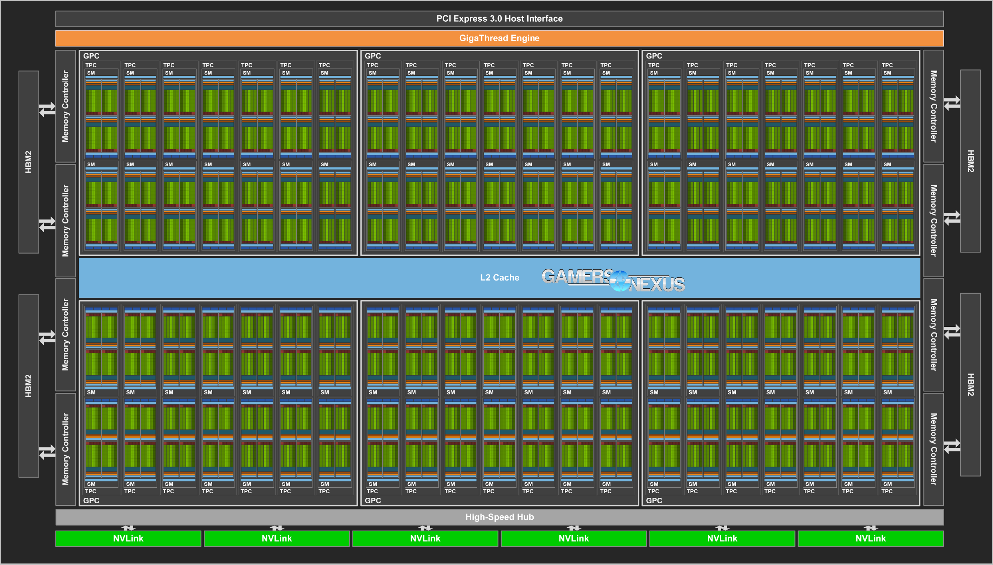
The Titan V reference PCB -- presumably the only PCB that will exist -- uses a 16-phase DrMOS VRM. The cooling solution is the same as used on the GTX 10 series of cards, including the 1080 Ti, and so uses a vapor chamber with radial blower fan. This matches the 250W TDP, as further reinforced by 1x 8-pin + 1x 6-pin power connectors. The cooler can't take much more than that, anyway. As for NVIDIA Titan V specs, the card is using a GV100 GPU with 5120 CUDA cores and 640 Tensor Cores, clocked to 1200MHz base / 1455MHz boost on the CUDA cores. The card also hosts 320 TMUs. Here is the block diagram from the original Volta announcement:
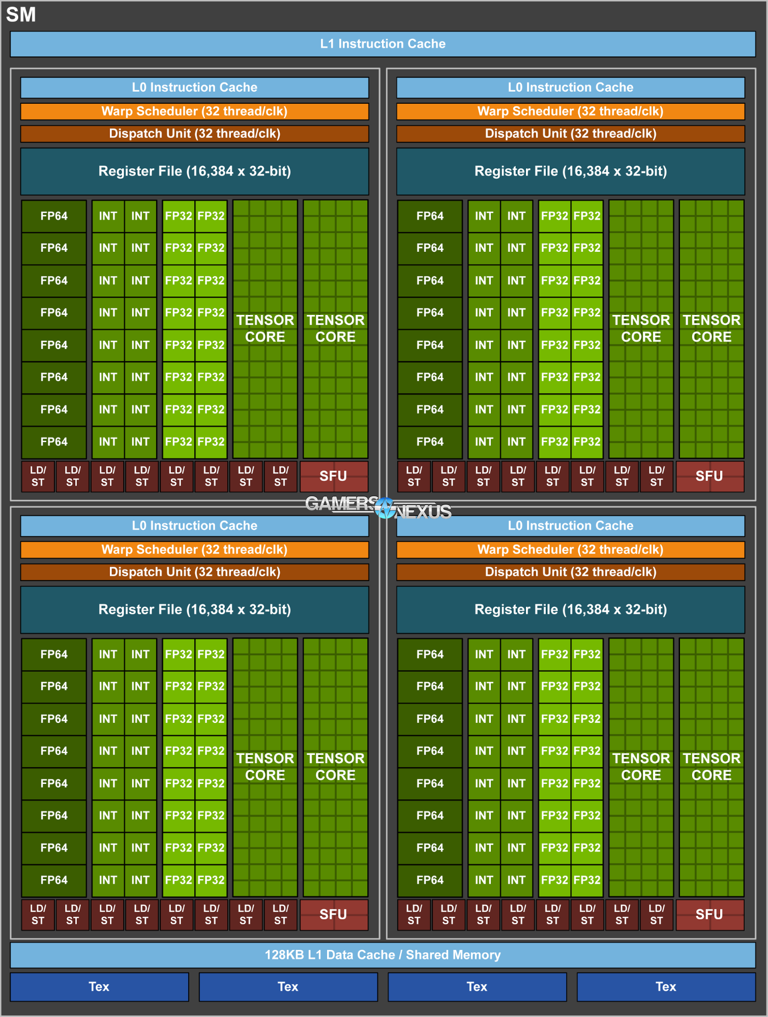
And here is the V100 SM block diagram from this year's Volta unveil in May:
- Steve Burke


