AMD’s got a new strategy: Don’t give anyone time to blink between product launches. The company’s been firing off round after round of products for the past month, starting with Ryzen 7, then Ryzen 5, and now Polaris Refresh. The product cannon will eventually be reloaded with Vega, but that’s not for today.
The RX 500 series officially arrives to market today, primarily carried in on the backs of the RX 580 and RX 570 Polaris 10 GPUs. From an architectural perspective, there’s nothing new – if you know Polaris and the RX 400 series, you know the RX 500 series. This is not an exciting, bombastic launch that requires delving into some unexplored arch; in fact, our original RX 480 review heavily detailed Polaris architecture, and that’s all relevant information to today’s RX 580 launch. If you’re not up to speed on Polaris, our review from last year is a good place to start (though the numbers are now out of date, the information is still accurate).
Both the RX 580 and RX 570 will be available as of this article’s publication. The RX 580 we’re reviewing should be listed here once retailer embargo lifts, with our RX 570 model posting here. Our RX 570 review goes live tomorrow. We’re spacing them out to allow for better per-card depth, having just come off of a series of 1080 Ti reviews (Xtreme, Gaming X).
A Partner Launch: No Reference Cooler
This is a partner launch. There is no “reference” card this time around, despite rumors proliferated by less scrupulous websites, and there will therefore exist no reference cooler. Despite promises by some sites that the RX 500 cards would include dual axial fan coolers, that’s not what reality promises. AMD’s Scott Wasson (who visited us to talk VR benchmarking and other topics) noted that the RX 500 series is focused on AMD’s board partners, and so those partners will be responsible for cooling solutions.
That cleared up, here’s a look at the new specs table:
| RX 580 | RX 570 | |
| GCN | Gen4 | Gen4 |
| Manf Process | 14nm FinFET | 14nm FinFET |
| Die Size | 232mm^2 | 232mm^2 |
| Compute Units | 36 | 32 |
| Stream Processors | 2304 | 2048 |
| Base/Boost | 1257/1340MHz | 1168/1244MHz |
| COMPUTE Peak | 6.17TFLOPs | 5.1TFLOPs |
| TMUs | 144 | 128 |
| Texture Fill-Rate | 193GT/s | 159.2GT/s |
| ROPs | 32 | 32 |
| Pixel Fill-Rate | 42.9GP/s | 39.8GP/s |
| Memory Config | 8GB 4GB GDDR5 | 4GB GDDR5 |
| Memory Bandwidth | 256GB/s | 224GB/s |
| Memory Interface | 256-bit | 256-bit |
| Board TDP | 185W | 150W |
The difference with the 500 series is effectively a pre-overclock, with some power tuning for low-load & idle tasks. The RX 580 and 570 cards ship with a higher native clock than previous reference clocks (and higher than most previous AIB partners), with additional OC headroom afforded through new voltage budget increases. Voltage can now be incremented an additional 25mV via Wattman, providing a total of 1200mV via the utility, plus whatever offset the board partners provide. In the case of MSI, we can get up to 1.256v on the MSI RX 580 Gaming X board, allowing a higher stable OC than the RX 480 card. We’ll look at our OC stepping table a bit later.
There’s a bit of a dichotomy in power behavior with the RX 500 series: More mature process means better efficiency, aided in some ways by nondescript “fine-tuning” done by AMD. These efforts bring the RX 500 series cards down in idle power consumption and low-load power consumption (like video playback). Naturally, power draw also increases at the high-end of the scale, as the higher frequency and voltage drink more from the wall. Power draw gets worse toward the top-end of the volt-frequency curve, given usual leakiness at the high-end, but tend to be better than the 400 series at the absolute low-end of that same curve.
For prices of the RX 500 series, here’s what we’ve got so far:
ASUS
- $189 for RX 570 STRIX OC 4GB
- $179 for RX 570 STRIX 4GB
Gigabyte
- $259 for RX 580 Aorus OC 8GB
- $229 for RX 580 Aorus 8GB
- $219 for RX 580 Gaming 8GB
- $199 for RX 580 Aorus 4GB
- $189 for RX 580 Gaming 4GB
- $179 for RX 570 Aorus 4GB
- $169 for RX 570 Gaming 4GB
MSI
- $245 for RX 580 Gaming 8G
- $229 for RX 580 ARMOR 8G
- $199 for RX 580 ARMOR 4G
- $175 for RX 570 ARMOR 4G
Sapphire
- $275 for RX 580 Nitro+ Limited edition 8GB
- $249 for RX 580 Nitro+ 8GB
- $229 for RX 580 Pulse 8GB
- $209 for RX 580 Pulse 4GB
- $199 for RX 570 Nitro+ 4GB
- $169 for RX 570 Pulse 4GB
TUL
- $269 for RX 580 8GB Red Devil Golden Sample
- $249 for RX 580 8GB Red Devil
- $229 for RX 580 8GB Red Dragon
- $199 for RX 580 4GB Red Dragon
- $175 for RX 570 4GB Red Dragon
We’re working with the MSI RX 580 Gaming today, priced at $245. For our core competing product, we’ll be re-testing the EVGA GTX 1060 SSC (priced at $240-$250 – i.e. equally). Some of the charts will allow an MSI 1060 Gaming X to pop-up, but it’s primarily between the RX 580 Gaming & EVGA 1060 SSC cards. We’ve got the RX 480 Gaming X on the charts as well, since it’s worth seeing whether the 580 posts any meaningful improvement over an overclocked 480.
For what it’s worth, we’ve also got a $250 XFX GTR unit and will review that posthaste. Our RX 570 is the Aorus 4GB model, priced at $180. The new price floor for the RX *70 series seems to be ~$170, continuing AMD’s already-competitive positioning against the 1050 Ti.
Refresher on Polaris Architecture
If Polaris is new to you – or if it’s just been a minute – here are some content pieces from the architecture’s debut:
To recap the basics, we’ll quote the first article:
“AMD has coupled its FinFET process with datapath organization improvements and improved data compression, both of which reduce overall power consumption. Memory alone has seen an energy reduction upwards of 40% per bit transacted, significantly lowered versus Hawaii and previous generations. This allows more room for energy provided to the cores, of course, but also reduces total consumption. Changes to boosting functions have also improved power utilization, mainly by introducing 7 DPM states (DPM1=sleep, DPM7=fully unlocked for high-end production/gaming).
“Clock gating and power gating for under-utilized circuits furthers the perf/watt argument, as does the introduction of heuristic pre-fetch routines that keep cycles occupied with instructions.
“But that's getting ahead of the architecture discussion.
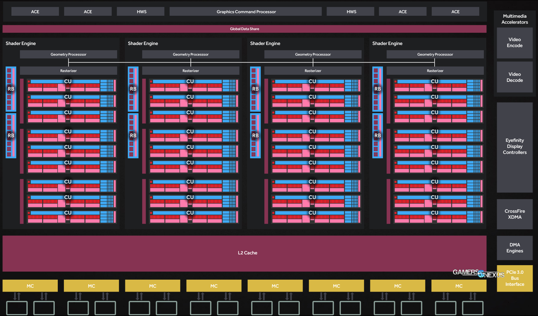
“Packed into the RX 480 Polaris 10 chip is a grouping of 36 CUs, over which rests a single GCP (Graphics Command Processor), flanked by two Hardware Schedulers (HWS) and four Asynchronous Compute Engines (ACEs). Polaris 10 and Polaris 11 both operate on a single GCP and have expanded reliance upon the HWS over what was found in Gen 3 GCN. The HWS block was first introduced on Gen 3, and owners of Fury- and 390-class GPUs will be happy to know that microcode updates to firmware will enable some of the Polaris-class HWS enhancements. One of those is the introduction of QRQs, which aid in hardware power reductions when using the Oculus Rift HMD. The HWS is controlled by microcode and can be updated through drivers, beneficial as hardware and APIs mature.
[…]
“One of the RX 480's biggest changes is its doubling of L2 Cache. With more capacity in cache for data storage, texture references and color compression remain resident for longer (reducing computational workload). This improves processing efficiency and reduces bandwidth consumption where unnecessary. There's no reason to transact the same data back-and-forth if it can be stored into a local, nearby cache.
“Critically, this also has a side effect which is perhaps overlooked: Energy savings. Along with the power reduction native to smaller FinFET process nodes – moving away from planar helps tremendously – the caching system reduces power consumed by GPU memory. Delta Color Compression (DCC) and 2MB of L2 Cache work in conjunction to minimize VRAM activity, and while it is impossible for us to test something this low-level at GN, AMD tells us that power savings are upwards of 40% on memory transactions alone.”
To read the rest on Polaris architecture, check page 1 of our original review.
MSI RX 580 Tear-Down
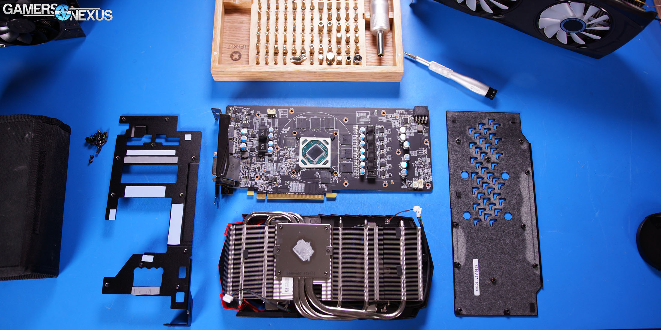
The MSI RX 580 Gaming is trivial to tear-down. It’s a couple screws in the back-side to secure a thermally functionless backplate to the card (if anything, it’s there for structural support), then four screws to release the finstack. Flipping the card over, three cables are responsible for fan and LED connections, with another two screws mounted into the backplate.
Under all this, an inscriptionless die is revealed and flanked by Samsung memory modules (K4G80325FB-HC). OnSemi M3816N power stages are used as part of the 6-phase VRM.
Before the Tests: Overclock Stepping
Before getting into power, thermals, and gaming benchmarks, we should probably show our work for overclocking. The charts will refer to an RX 580 “OC” – the below is what we’re talking about:
| Peak Clock (MHz) | AVG Clock (MHz) | Core Offset (MHz) | MEM CLK (MHz) | MEM Offset (MHz) | MEM mV | Power Target % | Voltage | mV | Fan | TMP | Pass/Fail |
| 1367 | 1344 | 0 | 2025 | 0 | 950 | 100 | 1.22 | Auto | 1600 | 72 | P |
| 1393 | 1393 | 0 | 2025 | 0 | 950 | 150 | 1.22 | Auto | 1860 | 72 | P |
| 1410 | 1410 | 15 | 2025 | 0 | 950 | 150 | 1.256 | 1150 | 1920 | 69 | P |
| 1420 | 1420 | 25 | 2025 | 0 | 950 | 150 | 1.256 | 1150 | 1920 | 68 | P |
| 1430 | 1430 | 35 | 2025 | 0 | 950 | 150 | 1.256 | 1150 | 1920 | 69 | Flicker |
| 1430 | 1430 | 35 | 2025 | 0 | 950 | 150 | 1.256 | 1180 | 1920 | 71 | P |
| 1440 | 1440 | 45 | 2025 | 0 | 950 | 150 | 1.256 | 1180 | 1920 | 71 | P |
| 1460 | 1460 | 65 | 2025 | 0 | 950 | 150 | 1.256 | 1180 | 2100 | 71 | Flicker |
| 1460 | 1460 | 65 | 2025 | 0 | 950 | 150 | 1.256 | 1200 | 2200 | 71 | Flicker |
| 1465 | 1465 | 70 | 2025 | 0 | 950 | 150 | 1.256 | 1200 | 2200 | 71 | Driver crash |
| 1455 | 1455 | 60 | 2025 | 0 | 950 | 150 | 1.256 | 1200 | 2200 | 71 | P |
| 1455 | 1455 | 60 | 2100 | 100 | 950 | 150 | 1.256 | 1200 | 2250 | 71 | P |
| 1455 | 1455 | 60 | 2200 | 200 | 950 | 150 | 1.256 | 1200 | 2250 | 71 | P |
| 1455 | 1455 | 60 | 2250 | 250 | 950 | 150 | 1.256 | 1200 | 2250 | 71 | P |
(Max power draw peaked at ~290W for the above).
The RX 480 Gaming X got stuck around 1365-1375MHz with its more limited 1175mV offset.
For the GTX 1060 SSC, this is what we ran with:
| Peak Clock (MHz) | AVG Clock (MHz) | Core Offset (MHz) | MEM CLK (MHz) | MEM Offset (MHz) | Power Target | Voltage | Pass/Fail |
| 1962 | 1962 | 0 | 2003 | 0 | 100 | 1.043 | P |
| 1962 | 1962 | 0 | 2003 | 0 | 120 | 1.043 | P |
| 2050 | 2050 | 100 | 2003 | 0 | 120 | 1.043 | P |
| 2101 | 2101 | 150 | 2003 | 0 | 120 | 1.043 | P |
| - | - | 175 | 2003 | 0 | 120 | 1.043 | F - Driver crash |
| 2152 | 2152 | 175 | 2003 | 0 | 120 | 1.075 | Flicker |
| 2101 | 2101 | 150 | 2202 | 400 | 120 | 1.081 | P |
| 2114 | 2114 | 150 | 2250 | 500 | 120 | 1.081 | P |
| 2114 | 2101 | 150 | 2305 | 600 | 120 | 1.081 | P |
| 2114 | 2101 | 150 | 2330 | 650 | 120 | 1.081 | F - Flicker/crash |
| 2075 | 2075 | 125 | 2250 | 500 | 120 | 1.081 | P |
Enough of this first page.
Continue to Page 2 for GPU test methodology.
GPU Testing Methodology
For our benchmarks today, we’re using a fully rebuilt GPU test bench for 2017. This is our first full set of GPUs for the year, giving us an opportunity to move to an i7-7700K platform that’s clocked higher than our old GPU test bed. For all the excitement that comes with a new GPU test bench and a clean slate to work with, we also lose some information: Our old GPU tests are completely incomparable to these results due to a new set of numbers, completely new testing methodology, new game settings, and new games being tested with. DOOM, for instance, now has a new test methodology behind it. We’ve moved to Ultra graphics settings with 0xAA and async enabled, also dropping OpenGL entirely in favor of Vulkan + more Dx12 tests.
We’ve also automated a significant portion of our testing at this point, reducing manual workload in favor of greater focus on analytics.
Driver version 378.78 (press-ready drivers for 1080 Ti, provided by nVidia) was used for all nVidia devices. Version 17.10.1030-B8 was used for AMD (press drivers).
A separate bench is used for game performance and for thermal performance.
Thermal Test Bench
Our test methodology for the is largely parallel to our EVGA VRM final torture test that we published late last year. We use logging software to monitor the NTCs on EVGA’s ICX card, with our own calibrated thermocouples mounted to power components for non-ICX monitoring. Our thermocouples use an adhesive pad that is 1/100th of an inch thick, and does not interfere in any meaningful way with thermal transfer. The pad is a combination of polyimide and polymethylphenylsiloxane, and the thermocouple is a K-type hooked up to a logging meter. Calibration offsets are applied as necessary, with the exact same thermocouples used in the same spots for each test.
Torture testing used Kombustor's 'Furry Donut' testing, 3DMark, and a few games (to determine auto fan speeds under 'real' usage conditions, used later for noise level testing).
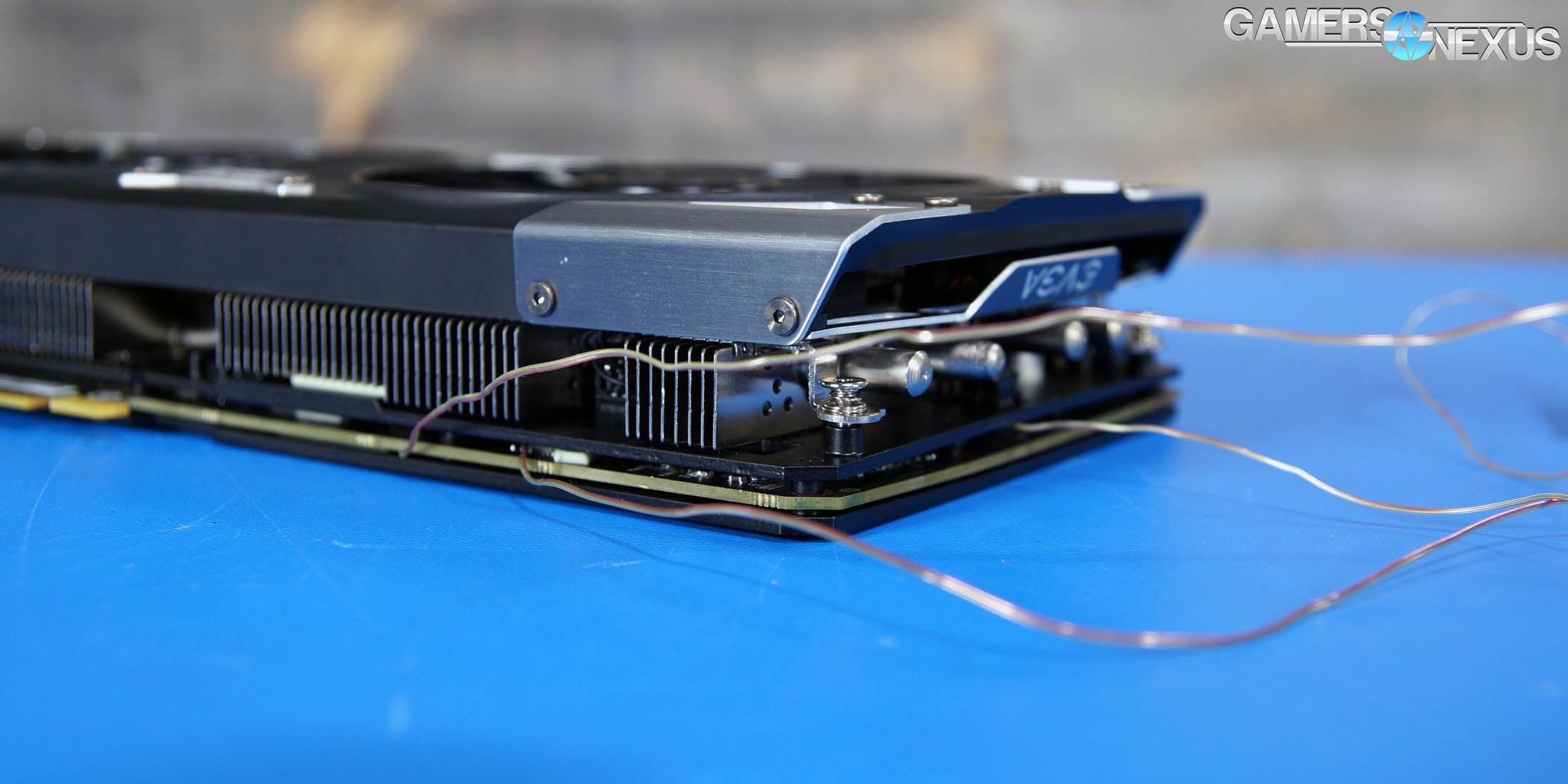
Our tests apply self-adhesive, 1/100th-inch thick (read: laser thin, does not cause "air gaps") K-type thermocouples directly to the rear-side of the PCB and to hotspot MOSFETs numbers 2 and 7 when counting from the bottom of the PCB. The thermocouples used are flat and are self-adhesive (from Omega), as recommended by thermal engineers in the industry -- including Bobby Kinstle of Corsair, whom we previously interviewed.
K-type thermocouples have a known range of approximately 2.2C. We calibrated our thermocouples by providing them an "ice bath," then providing them a boiling water bath. This provided us the information required to understand and adjust results appropriately.
Because we have concerns pertaining to thermal conductivity and impact of the thermocouple pad in its placement area, we selected the pads discussed above for uninterrupted performance of the cooler by the test equipment. Electrical conductivity is also a concern, as you don't want bare wire to cause an electrical short on the PCB. Fortunately, these thermocouples are not electrically conductive along the wire or placement pad, with the wire using a PTFE coating with a 30 AWG (~0.0100"⌀). The thermocouples are 914mm long and connect into our dual logging thermocouple readers, which then take second by second measurements of temperature. We also log ambient, and apply an ambient modifier where necessary to adjust test passes so that they are fair.
The response time of our thermocouples is 0.15s, with an accompanying resolution of 0.1C. The laminates arae fiberglass-reinforced polymer layers, with junction insulation comprised of polyimide and fiberglass. The thermocouples are rated for just under 200C, which is enough for any VRM testing (and if we go over that, something will probably blow, anyway).
To avoid EMI, we mostly guess-and-check placement of the thermocouples. EMI is caused by power plane PCBs and inductors. We were able to avoid electromagnetic interference by routing the thermocouple wiring right, toward the less populated half of the board, and then down. The cables exit the board near the PCI-e slot and avoid crossing inductors. This resulted in no observable/measurable EMI with regard to temperature readings.
We decided to deploy AIDA64 and GPU-Z to measure direct temperatures of the GPU and the CPU (becomes relevant during torture testing, when we dump the CPU radiator's heat straight into the VRM fan). In addition to this, logging of fan speeds, VID, vCore, and other aspects of power management were logged. We then use EVGA's custom Precision build to log the thermistor readings second by second, matched against and validated between our own thermocouples.
The primary test platform is detailed below:
| GN Test Bench 2015 | Name | Courtesy Of | Cost |
| Video Card | This is what we're testing | - | - |
| CPU | Intel i7-5930K CPU 3.8GHz | iBUYPOWER | $580 |
| Memory | Corsair Dominator 32GB 3200MHz | Corsair | $210 |
| Motherboard | EVGA X99 Classified | GamersNexus | $365 |
| Power Supply | NZXT 1200W HALE90 V2 | NZXT | $300 |
| SSD | OCZ ARC100 Crucial 1TB | Kingston Tech. | $130 |
| Case | Top Deck Tech Station | GamersNexus | $250 |
| CPU Cooler | Asetek 570LC | Asetek | - |
Note also that we swap test benches for the GPU thermal testing, using instead our "red" bench with three case fans -- only one is connected (directed at CPU area) -- and an elevated standoff for the 120mm fat radiator cooler from Asetek (for the CPU) with Gentle Typhoon fan at max RPM. This is elevated out of airflow pathways for the GPU, and is irrelevant to testing -- but we're detailing it for our own notes in the future.
Game Bench
| GN Test Bench 2017 | Name | Courtesy Of | Cost |
| Video Card | This is what we're testing | - | - |
| CPU | Intel i7-7700K 4.5GHz locked | GamersNexus | $330 |
| Memory | GSkill Trident Z 3200MHz C14 | Gskill | - |
| Motherboard | Gigabyte Aorus Gaming 7 Z270X | Gigabyte | $240 |
| Power Supply | NZXT 1200W HALE90 V2 | NZXT | $300 |
| SSD | Plextor M7V Crucial 1TB | GamersNexus | - |
| Case | Top Deck Tech Station | GamersNexus | $250 |
| CPU Cooler | Asetek 570LC | Asetek | - |
BIOS settings include C-states completely disabled with the CPU locked to 4.5GHz at 1.32 vCore. Memory is at XMP1.
We communicated with both AMD and nVidia about the new titles on the bench, and gave each company the opportunity to ‘vote’ for a title they’d like to see us add. We figure this will help even out some of the game biases that exist. AMD doesn’t make a big showing today, but will soon. We are testing:
- Ghost Recon: Wildlands (built-in bench, Very High; recommended by nVidia)
- Sniper Elite 4 (High, Async, Dx12; recommended by AMD)
- For Honor (Extreme, manual bench as built-in is unrealistically abusive)
- Ashes of the Singularity (GPU-focused, High, Dx12)
- DOOM (Vulkan, Ultra, 0xAA, Async)
Synthetics:
- 3DMark FireStrike
- 3DMark FireStrike Extreme
- 3DMark FireStrike Ultra
- 3DMark TimeSpy
For measurement tools, we’re using PresentMon for Dx12/Vulkan titles and FRAPS for Dx11 titles. OnPresent is the preferred output for us, which is then fed through our own script to calculate 1% low and 0.1% low metrics (defined here).
Power testing is taken at the wall. One case fan is connected, both SSDs, and the system is otherwise left in the "Game Bench" configuration.
Continue to Page 3 for thermals & power.
MSI RX 580 Thermals: VRAM, VRM, & Silicon
Our thermal test methods are defined on the previous page, where we talk about how the FET, VRAM, & PCB backside temperatures are measured. These are the same methods we’ve deployed and refined since our EVGA VRM analysis, and just recently used to analyze the three 1080 Ti cards we’ve reviewed of late.
Ambient runs 26.6-28.6C during this test, but we actively measure ambient and apply calculations to offset competing numbers in comparative charts.
The first chart looks at GPU diode, FET4 (fourth from bottom), and VRAM temperatures (middle-right module) to better understand the cooling capabilities of the MSI Twin Frozr cooler on this card. It’s not the most impressive cooling solution we’ve seen, but there’s still contact via thermal pad to the heatsink from all core components. FET#4 was chosen as it is the center of the VRM, and so should run the hottest by nature of being surrounded by other hot components. We’ve selected the middle-right VRAM module for this same reason – that tends to be where temperatures run high, given the proximity of the inductors and capacitor bank.
Here’s the first chart:
Everything’s fairly tightly packed. After an extended torture test in a power virus scenario, we rapidly learn that the fan profile is built to keep the RX 580 Gaming card’s GPU temperature to 70C, with frequency gating occurring alongside fan speed spikes to sustain that temperature. The VRAM module runs around 68-70C, the middle of the VRM (MOSFET4) runs around 70C, and the back plate sees a dip in temperatures as the fans continue their ramping process.
MSI RX 580 Clock Stability vs. Temp, Time, & Fan
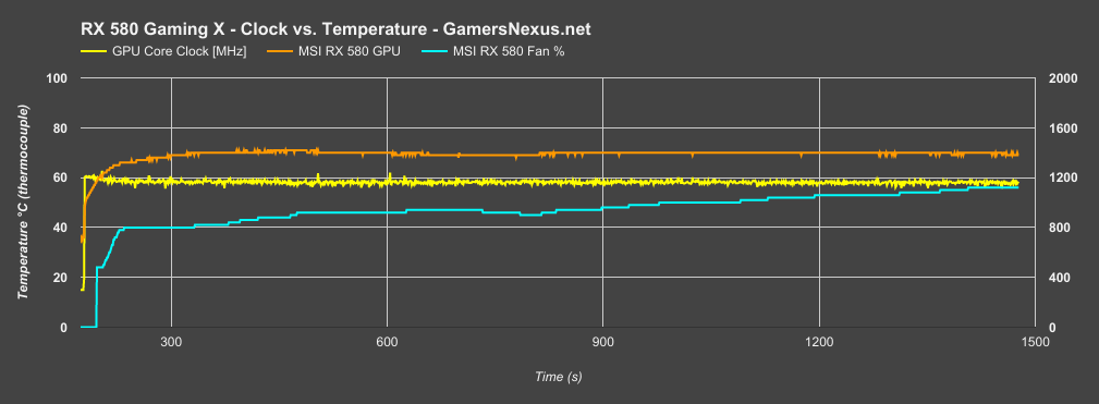
Above is the frequency vs. time and fan speed chart, which doubles somewhat as an indicator of temperature vs. noise (we won’t have time to run noise tests in time for this review, and will instead stick those into our XFX RX 580 review).
Clock dithering isn’t bad here, considering we’re just running the stock 100% power target. The frequency range is not greater than ~75MHz at worst, with most fluctuations sticking closer to 25-50MHz. This limits the impact to frametimes in later testing, though we’re contingent on drivers and other actors as well.
The MSI RX 580 Gaming is an interesting duck when it comes to its fan profile, though. For the most part, the card would have you believe the default profile is to stick around 50% -- but it just keeps steadily increasing, eventually stopping around 60%. The curious part is just how long MSI drags-out this ramp-up process. We tend to see most fan profiles peak within 10 minutes of this test, and so a ~20-minute run is sufficient to see the fan profile’s full behavior. MSI pushes to about 60%, just over a long period. To the cooler’s credit, it was able to maintain the 70C target temperature throughout the test, with only a few spikes (which align with frequency dips, if you hadn’t noticed).
AMD RX 580 Power Draw (Gaming X) vs. GTX 1060 (SSC)
Power has a direct correlation with thermals, and so it’s important to establish a baseline power measurement in some real use cases. Our power testing is done at the wall, which means this is a measurement of total system power draw and not individual GPU draw. We mostly care about the card-to-card deltas, here. This is an imperfect means of measuring component-level power draw, but a functional solution for the basics (ideally, we’d measure at the rails to determine PCIe compliance, but we’re not there yet).
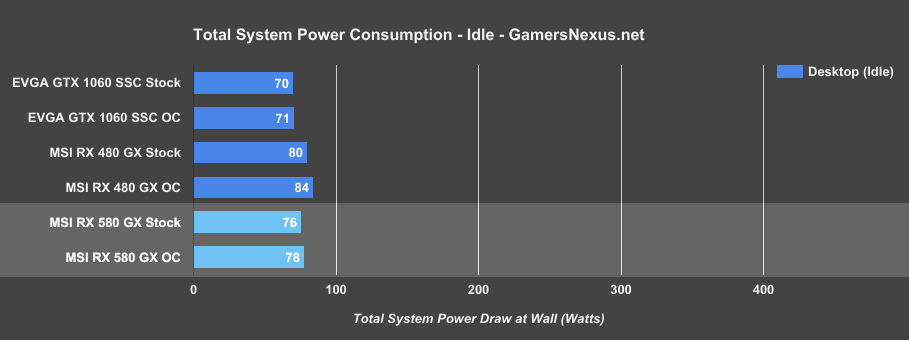
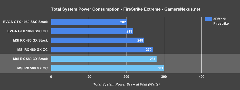
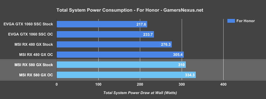
For the power tests, we’re using two games configured to Very High & Extreme graphics settings (1440p), 3DMark FireStrike Extreme, and idle draw at desktop.
Idle, the RX 580 Gaming system consumes about 76W, which is a reduction of a few Watts from the RX 480 stock configuration. This is expected: AMD’s tuning on its 14nm process has brought down power consumption when idle and when viewing movies or performing other low-load tasks. The RX 580 system draws about 8.6% more power idle than the 70W 1060 system.
3DMark FireStrike posts the RX 580 Gaming X stock system at 281W, with the overclocked variant – now pushing 1.26v – at 301W. That’s a total increase in power consumption of 7%. The RX 480 Gaming X system draws 248W, with its overclocked counterpart at 270W when running 1375MHz on the core. The RX 580 Gaming X consumes approximately 13% more power than the RX 480 Gaming X when both are stock. The EVGA GTX 1060 SSC runs the same workload with a total system draw of 202W stock, or 219W overclocked. The RX 580 consumes approximately 39% more power than the GTX 1060 SSC.
For Honor is one of our more load-intensive games, landing the 580 systems at 310W stock, or 334W overclocked, for an increase in power consumption of about 12% over the RX 480. The 1060 SSC runs around 218W stock and 234 OC, resulting in the RX 580 consuming about 42% more power when both are stock.
Ghost Recon shows more of the same.
Continue to Page 4 for synthetic benchmarks.
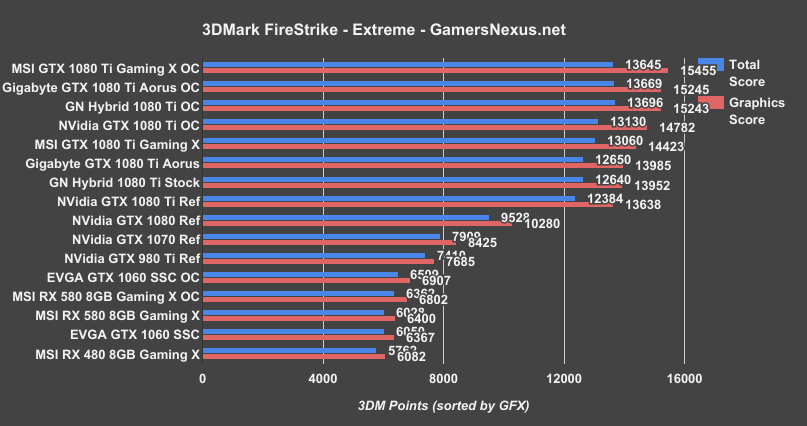
We dedicate our analytical efforts to real-world gaming, power, and thermal benchmarks. As such, 3DMark is thrown-in more to provide a staple to benchmarkers and enthusiasts, and less for analysis. We provide the 3DM benchmark charts as-is – continue to the gaming page for conclusions and analysis, though.
3DMark – Firestrike (normal), 3DMark – Firestrike (Extreme – 1440p), and 3DMark – Firestrike (Ultra – 4K) are included in these tests. We also run Timespy for a Dx12 synthetic mark.
Continue to Page 5 for the gaming benchmarks & conclusion.
Mass Effect: Andromeda – RX 580 vs. RX 480, GTX 1060
Starting with Mass Effect: Andromeda at 1080p, the RX 580 Gaming X stock card runs an average framerate of about 79FPS, with 1% lows at 62 and 0.1% lows at 57FPS. Frametimes here are relatively consistent and in-line with other results. Versus the stock RX 480 Gaming X, this is an improvement of about 5.4% stock, or about 6.8% when looking at the overclocked RX 580 versus the overclocked RX 480. The overclocked RX 580 outperforms the Fury X in this particular test, and performs about 2.4% behind the GTX 970 or 7% behind the GTX 1060 SSC, which operates framerates of 89, 68, and 64. Overclocking the GTX 1060 SSC gets it to 95FPS AVG, just ahead of the GTX 1060 Gaming X from MSI. The overclocked RX 580 performs about 13% behind the overclocked GTX 1060 SSC, with the stock RX 580 performing about 11% behind the stock GTX 1060 SSC. Strictly for point of reference, the RX 470 runs at around 63FPS in this test, the R9 390X at about 70, and the GTX 1070 SC at about 119FPS.
Here's a look at the stock clock frametimes of the RX 580 versus the GTX 1060 SSC, just to help give an idea of latency between frames.
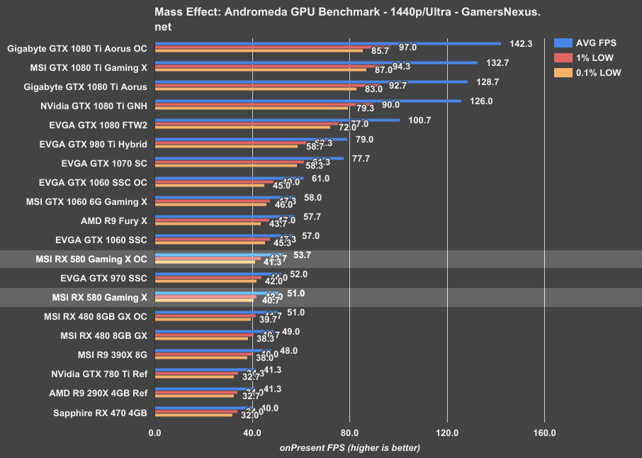
Moving to 1440p, the RX 580 Gaming X stock is now running at 51FPS AVG, with the same consistent frametimes as most other results in the stack. The stock RX 580 is evenly matched with our overclocked RX 480 Gaming X, or about 4% ahead of the stock RX 480. The RX 580 OC operates about 5.3% faster than the stock version, now at 54FPS AVG, which leaves the 580 cards flanking the GTX 970.
Looking to the direct competitors in the GTX 1060 class, the SSC stock runs at 57FPS AVG, putting it about 16% ahead of the stock RX 580, with the overclocked SSC card running around 13.6% ahead of the overclocked RX 580.
Ghost Recon: Wildlands – AMD RX 580 8GB vs. GTX 1060 6GB, RX 480
Time to move on to Ghost Recon: Wildlands, then we’ll get to DOOM with Vulkan.
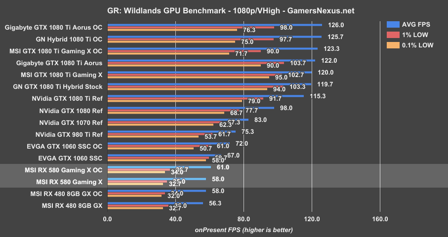
At 1080p, the RX 580 Gaming X lands at 58FPS AVG, roughly the same as the RX 480 Gaming X – the difference is in the frametimes, though. We’re seeing better frametimes on the RX 580 Gaming X, as shown in this frametime plot of the two Polaris cards against each other.
As for the GTX 1060 SSC, the Pascal card lands at 67FPS AVG stock, marking it in a lead of about 15.5%. Overclocking the 1060 SSC gives it some trouble in the 0.1% department, but we see a boost to 72FPS AVG. The 580 Gaming X moves to 61FPS AVG.
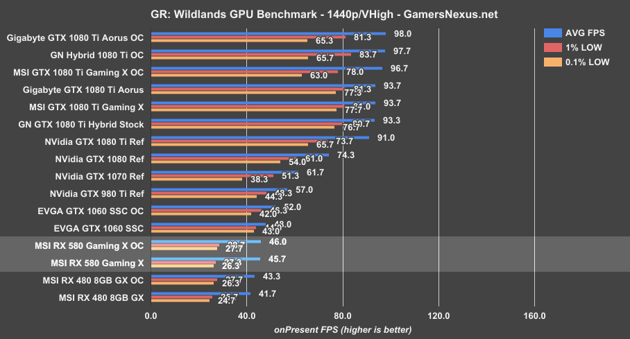
Moving on to 1440p, the RX 580 Gaming X runs around 46FPS AVG, with the GTX 1060 SSC at 48FPS AVG. Increasing the resolution has shrunken the gap between the devices, with the 1060 SSC primarily pulling away when overclocking.
DOOM (Vulkan) – AMD RX 580 vs. RX 480, GTX 1060
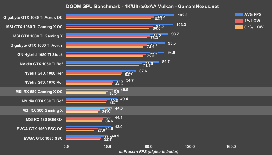
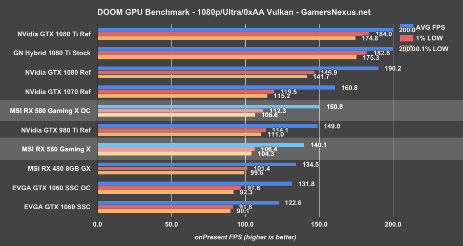
Now moving to DOOM at 4K, the RX 580 Gaming X lands at around 44FPS AVG alongside the RX 480 Gaming X, just behind the 980 Ti and just ahead of the GTX 1060 SSC. The RX 580 stock leads the EVGA 1060 SSC stock by about 8.3%, with the overclocked SSC showing some stability issues in its frametime consistency. The RX 580 overclocked gets up to 50FPS, an improvement over the stock 580 of about 11.7%.
Let’s move on to a more realistic resolution of 1440p.
The RX 580 Gaming X stock card runs around 91FPS AVG, again posting an uninteresting 1.5% climb from the RX 480’s position. The 580 stock outperforms the 1060 SSC by about 12%, with the 1060 SSC running at 81FPS AVG and with similar frametimes and lows to the 580 Gaming X. Overclocking the SSC gets it to 87FPS AVG, while the overclocked RX 580 Gaming X hits about 100FPS AVG at 1440p. The 580 OC leads the 1060 OC by about 15%.
Looking at 1080p, the RX 580 Gaming X runs at 140FPS AVG, with 1% lows at 106 and 0.1% lows at 104. The GTX 1060 SSC Stock runs 123FPS AVG, with lows at 92FPS and 90FPS. This puts the RX 580 stock in a lead of about 14.3%, with the overclocked 580 leading the overclocked SSC by about 14.4%.
For Honor – AMD RX 580 vs. GTX 1060, GTX 1070, RX 480
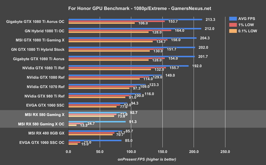
Playing For Honor at 1080p and with Extreme settings, the RX 580 Gaming X places at around 93FPS average, with frametimes tightly timed (reminder: we actually play the game rather than use the unrealistic bench tool). The GTX 1060 SSC performs similarly, running an average FPS of 94, with lows at 83 and 77 to the 580’s 77 and 73.
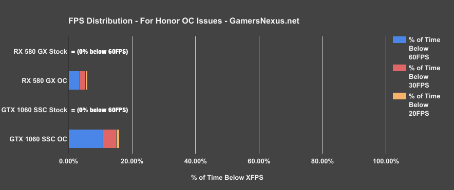
Overclocking in this game always goes over poorly unless we really minimize the OC. To get anything resembling stable on the GTX 1080 Ti Aorus card, we had to set the offset to just 20MHz. Not that impressive. Ignore the OC numbers here, as the game is unplayable and abnormally sensitive to overclocks. We’re just putting the numbers here so that this is understood; as you can see, both the 1060 and 580 are unplayable with their respective OCs.
Back to the focus of the chart: The 580 Gaming X is outperformed by the GTX 1060 SSC by about 1.7%, with the RX 580 Gaming X running about 8% faster than the RX 480 Gaming X.
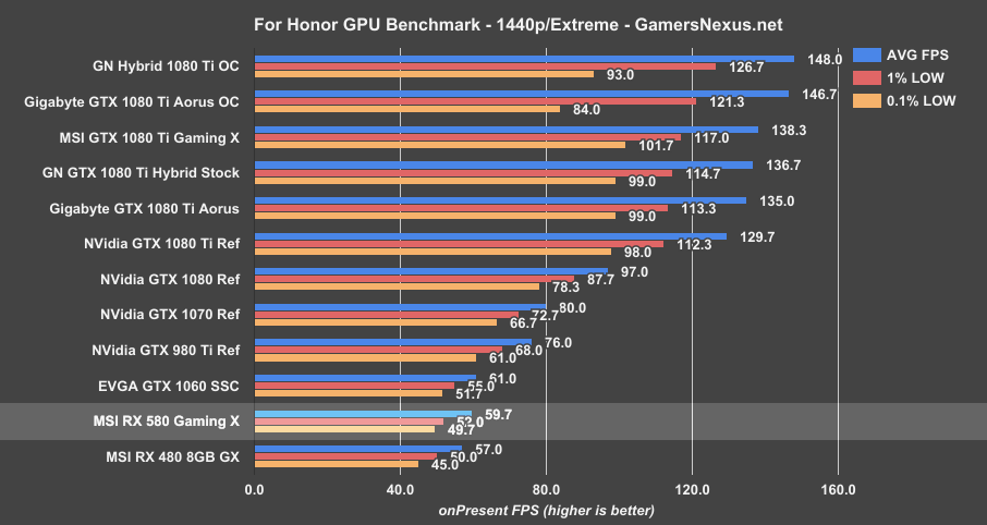
At 1440p, the RX 580 Gaming X runs a framerate of about 60FPS AVG, making it 4.7% faster than the RX 480’s 57FPS AVG. The GTX 1060 SSC operates at 61FPS AVG, leading the 580 by about 2.1%. Nothing significant or exciting between either device – they are both good performers when operating at stock frequencies in For Honor. They are imperceptibly different.
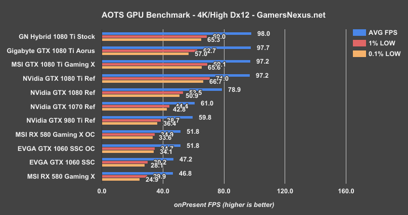
Ashes of the Singularity (Dx12) – AMD RX 580 vs. GTX 1060, 1070, RX 480
Sniper Elite 4 (Dx12) – MSI RX 580 Gaming X vs. GTX 1060 SSC
Sniper Elite 4 is our final game. We only currently have 4K numbers for this one, but we still get a good look at an intensive Dx12 scenario.
The RX 580 Gaming X runs at 40FPS AVG here, with the overclocked variant at 44FPS AVG. This puts the RX 580 Gaming X about 13-14% ahead of the 1060 SSC, both overclocked and stock. We’re trading blows between titles, it appears.
Conclusion
This isn’t something you buy if you already own Polaris or a 1060. These cards are meant for new builds – they’re not upgrades for anything recent. If you just bought an RX 480 and you’re feeling a little salty at the refresh, take solace in knowing that many of the games only post differences of 5% or thereabouts, if that. Overclocking will allow the RX 480 to mostly match an RX 580 stock card, since the stock card is just an RX 580 with a higher native frequency and more voltage to play with.
The GTX 1060 SSC and RX 580 Gaming X ($245) pass the trophy back-and-forth depending on the game, with nVidia generally looking good in Dx11 titles, while AMD does well in DOOM (expectedly) and Sniper Elite 4 (Dx12). Power consumption on the AMD card is significantly higher than the GTX 1060 SSC ($250), but the relevance of that change is up to the user. Of note, AMD did manage to bring its idle draw down from the RX 480 series, so that’s a strong positive since systems normally spend most their time idling.
With regard to pure gaming performance, the RX 580 competes well with the GTX 1060 SSC. They’re not that far apart in performance, and generally swap leadership on charts.
Nothing too exciting here, but not a bad launch. Just sort of a “meh” mid-cycle refresh that’s not particularly invigorating, but also worthwhile. The RX 580s we’ve seen thus far have a noteworthy increase in clock (which does benefit gaming), a lowered or equivalent price to previous cards, and retain competitive matchups with same-priced nVidia cards.
We’re most interested in the impending RX 570 analysis, though – the lowered price of the RX 570s (and increased performance) promise a reinforced hold over nVidia’s 1050 Ti. Last we checked, nVidia did best in the $100 market (with the 1050 outmatching the RX 460 in everything), AMD’s 470 tended to make more sense than the 1050 Ti, and the 1060 and RX 480 traded blows. The stack seems to be about the same, with the potential for the 500 series to shake-up the low-end and outpace the 1050. We’ll see how that goes, though; we’ve not yet received the low-end devices.
Editor-in-Chief: Steve Burke
Video Producer: Andrew Coleman
