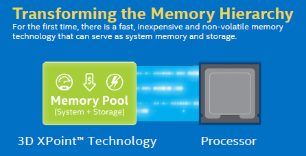
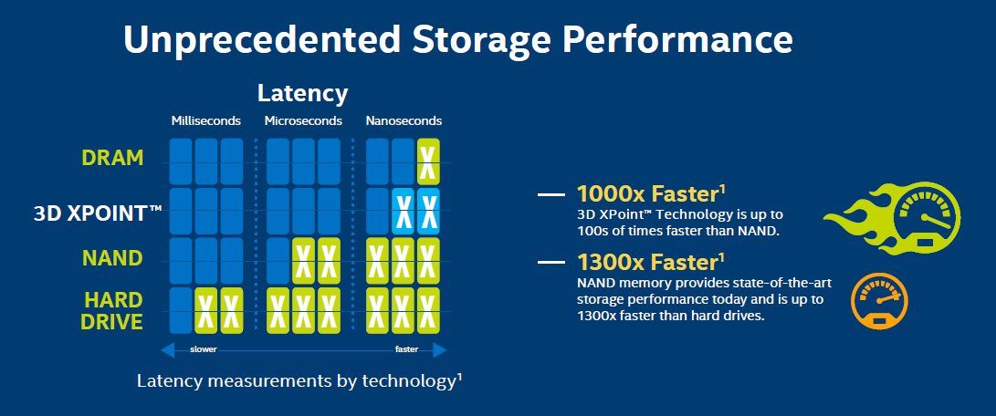
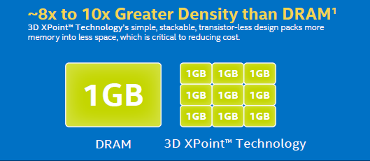
Optane is Intel’s latest memory technology. The long-term goal for Optane is for it to be used as a supplemental system memory, caching storage, and primary storage inside PCs. Intel claims that Optane is faster than Flash NAND, only slightly slower than DRAM, has higher endurance than NAND, and, due to its density, will be about half the cost of DRAM. The catch with all of these claims is that Intel has yet to release any concrete data on the product.
What we do know is that Lenovo announced that they will be using a 16GB M.2 Optane drive for caching in a couple of their new laptops during Q1 2017. Intel also announced that another 32GB caching drive should be available later in the year, something we’ve been looking into following CES 2017. This article will look into what Intel Optane actually is, how we think it works, and whether it's actually a viable device for the enthusiast market.
How Optane is Supposed to Work
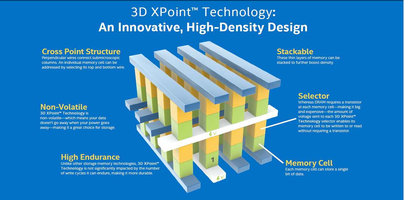
Intel and Micron have been working together to build Optane using what they call 3D Xpoint (cross-point) technology. As the name indicates, it’s a three dimensional structure providing non-volatile, bit-level memory access. In Intel’s words, they slice “submicroscopic layers of materials into columns, each containing a memory cell and selector, then [connect] them with an innovative cross-point structure of perpendicular wires."
As an alternative, one could think of it like this: The “perpendicular wires” are like addressing bars lying in parallel across a plane. Now, stack those planes one on top of the next creating a sort of tower. While keeping the addressing bars in their respective planes, rotate every layer 90° to the one below. Then, connect each layer with the vertical columns made up of the memory cells and selectors. This creates a cross connected, tower-like structure known as 3D Xpoint.
(From this point forward, we’re taking our best guess as to how it works due to the fact that Intel has to maintain its IP. The following explanations are based on a good amount of research from reputable sources. Without official documentation to reference, GN wants to make sure that its readers understand there could be inconsistency between the real thing and the explanation.)
The only thing left to explain now is how the data is written and read in 3d Xpoint technology. To address a memory cell, voltage is applied to the perpendicular conductors (bitline and wordline) adjacent to the memory cell. This triggers the selector portion of the column. Based on the voltage level, the selector allows either a read or a write. If the voltage is higher, then a write is issued and the resistive properties of the cell are altered to either a low resistance, probably reflecting a 0, or a high resistance reflecting a 1. If the selector senses a lower voltage, it probably permits the read action where the level of resistance is reported back to the system.
Assuming Optane turns out to be what Intel claims it is, enthusiasts will be one step closer to eliminating the PC storage bottleneck. We look forward to delving into the data from the drives as soon as we can get them. We’ll investigate where the latencies fall, if they’re as close to DRAM as Intel stated, or if they’re closer to that of NAND. We’ll also look forward to endurance data and, the clincher for many enthusiasts, how much the price per gigabyte will end up being.
- Patrick “Mocalcium” Stone


