This is primarily a video project that revisits our popular SSD Architecture post from 2014. All of that content remains relevant to this day – SSD architecture has not substantially changed at a low level – but it's been deserving of a refresh. NAND Flash comprises the actual storage component of the SSD, and impacts more than just capacity; endurance, speed, and the cost-per-GB metric are all impacted by NAND Flash selection. The industry has slowly reached parity between TLC and MLC NAND devices for the mainstream and gaming segments, with VNAND getting a steady push through Samsung's channels. As for how MLC and TLC actually work, though, we turn to our content.
With this update, we've introduced a 3D animation to help visualize the complexities of voltage states and program/erases occurring on the disk actively. The original graphics and text of our architecture article can be found on this page.
What is NAND Flash?
NAND Flash is a non-volatile, permanent memory. In this regard, NAND Flash on SSDs serves a similar purpose as the platters of a hard drive: It stores data with relative permanence, as opposed to volatile system memory which only temporarily stores data for recall. A hard drive, though, uses electromagnets and large, spinning platters with physically moving headers for data storage. There is a mechanical component to hard drives which governs their maximum operating speed – tied to the speed of the moving head (like a record player) – and increases noise/vibration with increases to maximum throughput.
NAND does not magnetically store its data; instead, NAND Flash takes the route of electrical read/write operations by checking voltage states. Each piece of data is transacted as a bit, and is stored at the 'cell' level within the SSD.
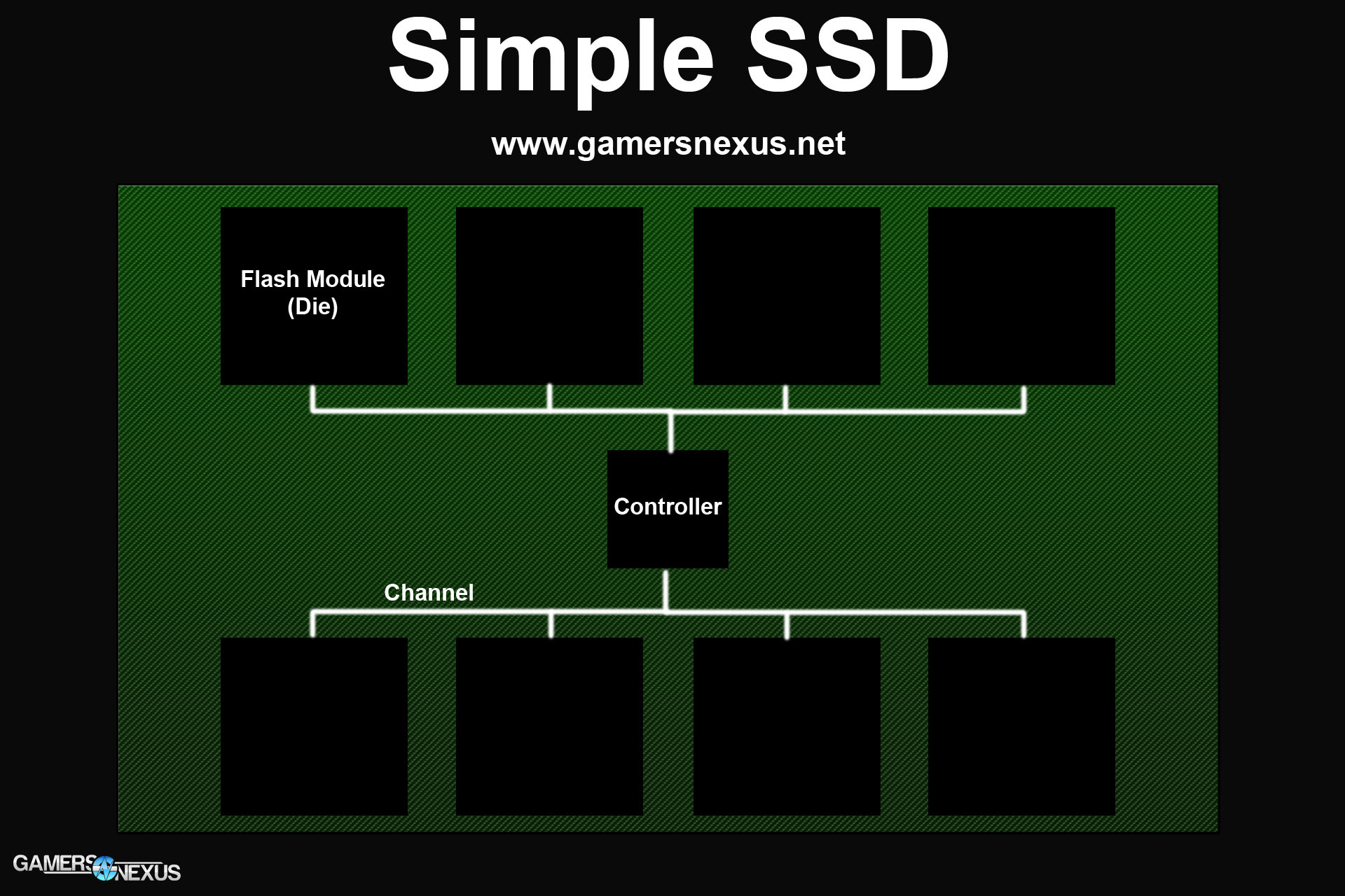
Here's a simplified SSD image we made for the 2014 article:
Our simplified SSD above is comprised of a controller – effectively the SSD's CPU, as it is more-or-less a small computer, eight channels, and eight flash modules that are connected to those channels. In this imaginary SSD, we have completely maxed-out our controller's available channels with flash modules.
The controller handles wear-leveling, garbage collection, extending P/E cycles, and governs Write Amplification Factor (WAF), all of which we've discussed in this previous content.
Focusing on the NAND, we might imagine that our sample SSD above uses 16nm MLC Flash NAND. The nm number is the process node for the silicon, as cut at the fabrication plant and supplied to SSD makers for use in their drives. “MLC” represents the NAND Type – multi-level cell, in this case. There are two bits of data per cell in this type of NAND, as opposed to single-bit storage on SLC and triple-bit storage on TLC. Let's look deeper:
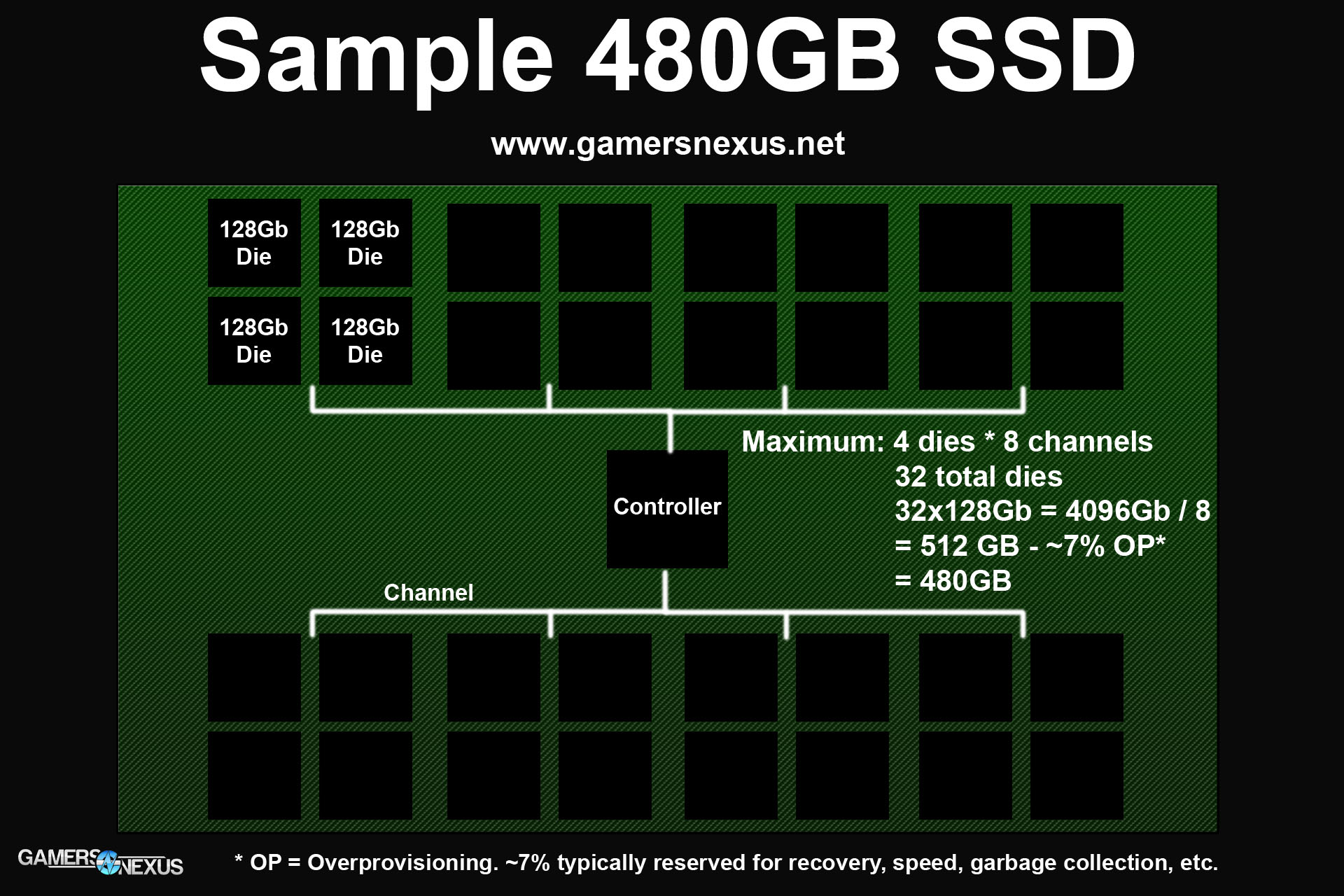
Each Flash module can contain multiple flash dies. In this example, we've shown the math behind how a 480GB or 512GB SSD might be created. Our sample NAND is 128Gb per module at four dies per module, and eight total modules. That's 32 dies at 128Gb, or 16GB each, totaling 512GB of storage. If you assume some normal amount of overprovisioning space – often about 7% – that puts us at a 480GB SSD.
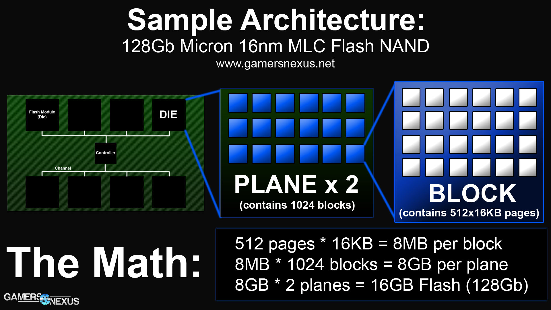
NAND is spliced into an organization structure to ensure the drive ages well. A Flash die consists of a few planes – normally two – which are then broken into blocks. Let's say there's 1024 of those, and then blocks contain pages. A page is the smallest unit of data storage on the SSD, generally 16KB in size, before going down to the cell level.
The SSD is split in this way because the controller moves data constantly to ensure all the blocks get worn-in equally. NAND Flash can only tolerate so many Programs – or writes – and so many erases before it expires and enters a read-only state. Collectively, program and erase actions are called P/E Cycles. If any block exhausts its P/E cycles unevenly, it could jeopardize the entire drive, so the controller works to wear-level the NAND at an equal rate. This means non-stop movement of data from cell-to-cell, based upon the user's (or host's) issued P/E requests.
In this regard, every time you write and erase data on your SSD, you're actively killing it. The process of wear-level and garbage collection have gotten sophisticated enough, in combination with high P/E cycle counts, that most users will exhaust the system's life before that of the SSD.
But there's more – let's look at cells.
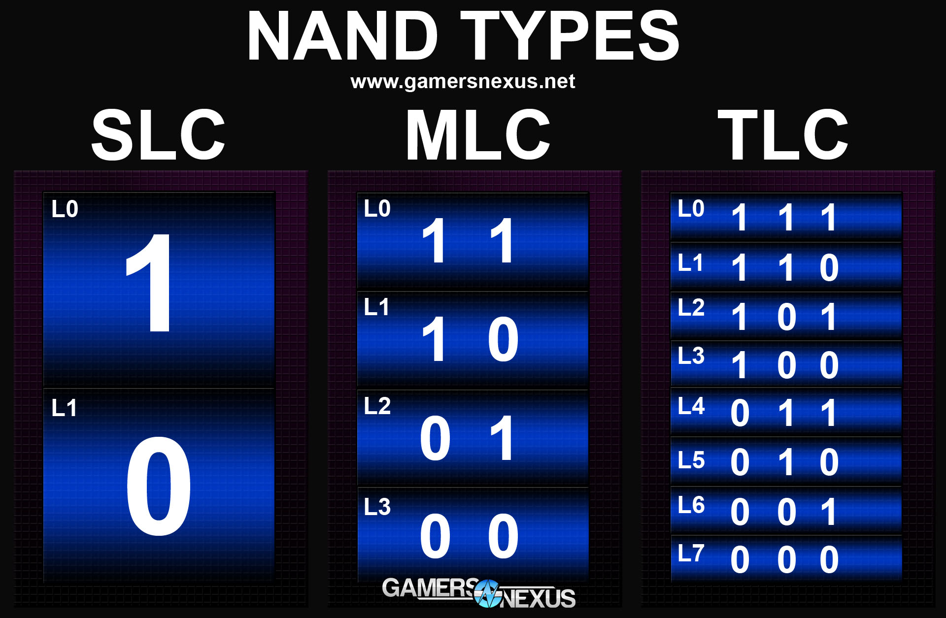
Cells work at the bit-level. There are billions of cells in every SSD, each responsible for its own bit or bits of data. SLC stands for single-level cell, MLC for multi-level cell – two levels, and TLC for triple-level cell.
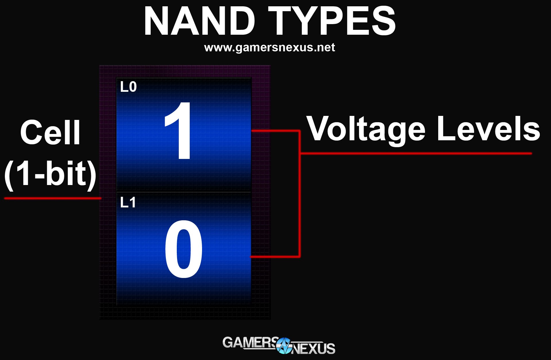
SLC NAND can contain only one bit of data per cell, so it's smaller in capacity per cell, but faster. There are only two possible voltage states for this cell: 1 or 0. When a charge is sent to the cell, it returns either a 1 or a 0 for the voltage check. A voltage check sees what data, if any, currently occupies a cell. Because there are only two possible voltage outcomes, the device runs with greater stability and performance than the more populated multi-level and triple-level cells, each of which stores exponentially more voltage levels and requires greater electrical precision at the time of checking. SSD aging sees a slow degradation in the electrical charge, which impacts accuracy of voltage checks on TLC and MLC NAND. Because SLC holds only two possible voltage states, it is less susceptible to bit errors during checks.
This also means that the SLC SSDs will be smaller in capacity and cost more, because twice the cells are required to achieve capacity parity with MLC, which stores two bits of data per cell and has four voltage levels. TLC contains three bits of data per cell – so it can hold ~30% more data per cell than MLC – but uses eight voltage levels. Cost per gigabyte drastically decreases with TLC and MLC, but there is a speed and endurance trade-off. SLC is mostly used for enterprise, though even that is becoming rare.
TLC has 7 readpoints between its voltage levels, MLC has three, and SLC has one. More readpoints means more space for data, but greater granularity required at the electrical level for voltage checks.
That covers the basics of NAND, but there's a lot more to it. The controller dictates a lot of the SSD's aging procedure, and advanced wear-leveling or WAF reduction can increase the endurance of even TLC enough to last a system lifetime.
Editorial: Steve “Lelldorianx” Burke
B-Roll: Keegan “HornetSting” Gallick
Video & Animation: Andrew “ColossalCake” Coleman
